Research Profile
Google Scholar
Total Citations: 17249
H-Index: 58
i10-index: 131
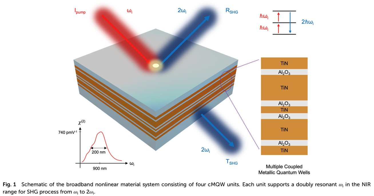
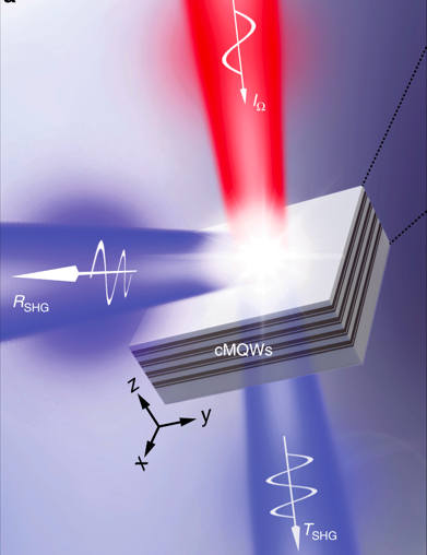
A material system with strong and broadband optical second-order nonlinearity in the near-infrared is theoretically and experimentally demonstrated. Multiple units of TiN-based coupled metallic quantum wells with slightly shifted nonlinear response peaks are uniquely designed and epitaxially grown to form a multilayered stack. By measuring near-infrared to visible second-harmonic generation, second-order susceptibility chi(2) reaches 740 pm V-1 at 900 nm and spreads 200 nm, covering the wavelength range from 800 nm to 1000 nm. Our discoveries open up the possibility to create materials with tailored optical nonlinearity, which can be valuable for building nonlinear optical devices in the fields of bioimaging, ultrafast light source generation, and quantum information technologies.
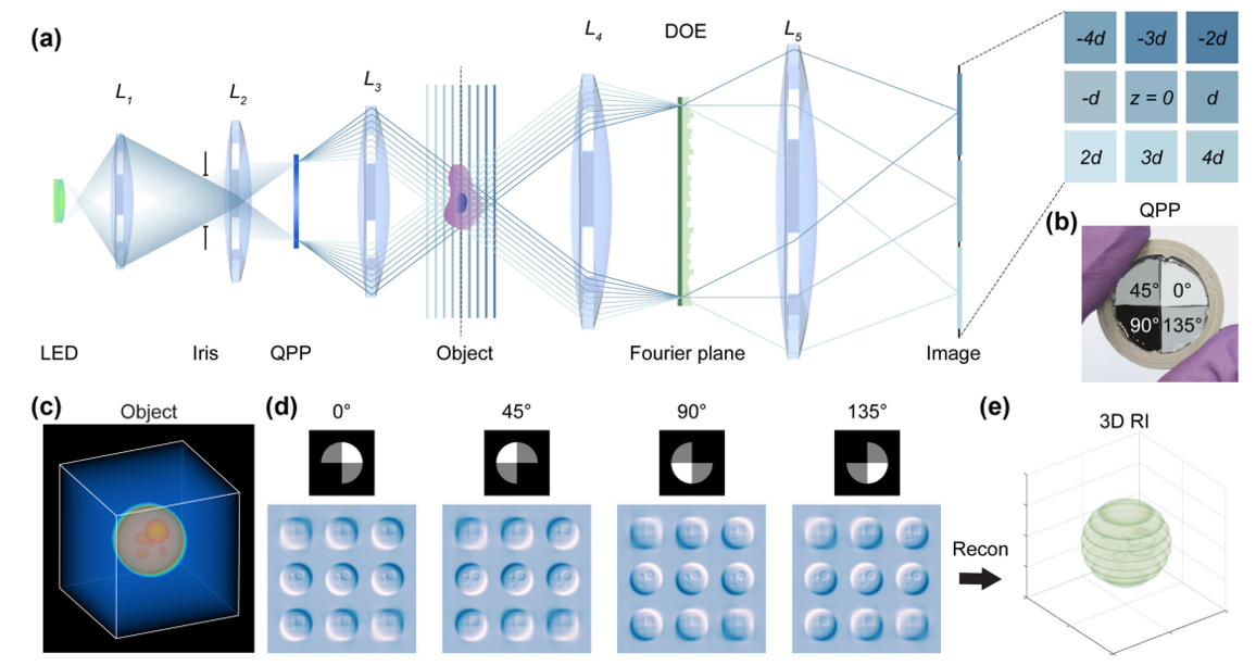
Phase Imaging enables label-free visualization of transparent biological samples, offering critical insight into cellular structure and transient dynamics with minimal phototoxicity. However, existing three-dimensional (3D) phase imaging techniques typically require sequential scanning or interferometric setups, limiting temporal resolution and increasing system complexity. To overcome these challenges, we propose snapshot parallel refractive index tomography (SPRIT), a snapshot, 3D refractive index (RI) imaging technique. SPRIT employs a diffractive optical element to capture multifocal intensity images. The volumetric RI distribution is reconstructed by deconvolving the intensity measurement with the 3D transfer functions of the system. By incorporating partially coherent illumination, SPRIT achieves higher spatial resolution than coherent imaging systems, with the degree of enhancement governed by the illumination and detection numerical apertures.We demonstrate volumetric imaging of liveChilomonas at 50 Hz with SPRIT, showcasing its ability to resolve fine subcellular structures in real-time. With its snapshot, high-resolution capabilities, SPRIT offers a powerful tool for label-free 3D imaging in cellular biology and medical diagnostics.
Blind structured illumination microscopy (blind-SIM) is a valuable tool for achieving super-resolution without the need for known illumination patterns. However, in its current formulation the algorithm requires many iterations to converge, leading to long inference times and limited use for real-time or video-rate imaging. We present unrolled blind-SIM (UBSIM), an algorithm which integrates a learnable neural network inside the unrolled iterations of the blind-SIM algorithm. UBSIM delivers a reconstruction speed two to three orders of magnitude faster than that of current iterative blind-SIM methods, while achieving similar resolution and image quality. Furthermore, we demonstrate that UBSIM can be trained in an unsupervised manner that reduces hallucinations and produces superior generalization capability when compared to benchmark super-resolution networks. We test UBSIM experimentally on live cells and present video-rate super-resolution imaging up to 50 Hz. Using our method, we observe dynamic remodeling of theendoplasmic reticulum with high spatiotemporal resolution.
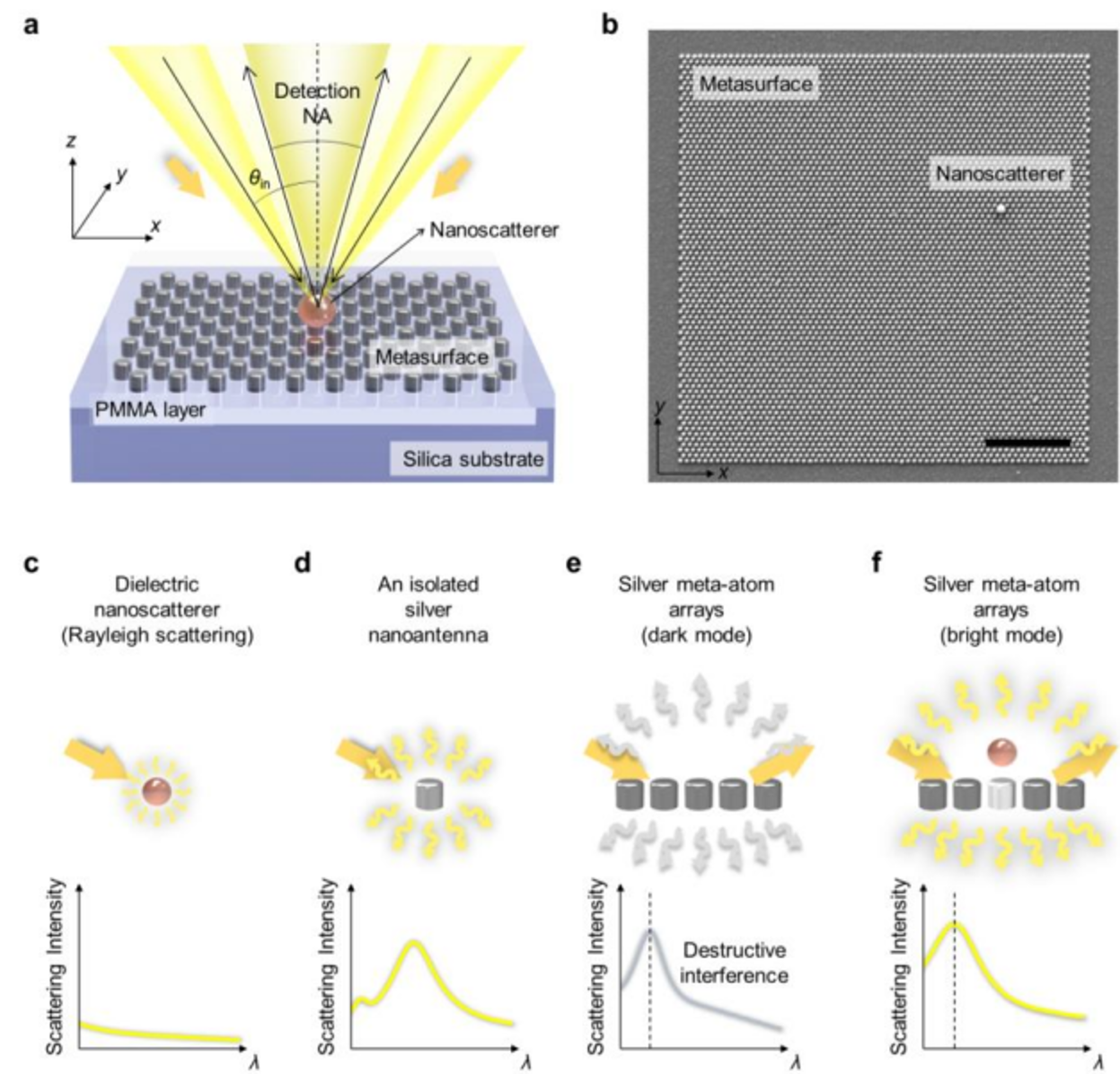
Label-free optical detection of nanometer-scale bioparticles is highly desirable for noninvasive biological studies but challenging due to the weak scattering signals that are difficult to distinguish from the illumination background. Interferometric scattering microscopy (iSCAT) has enabled high-sensitivity imaging by detecting the interference between the particle's scattered light and a reference beam. However, enhancing the detection sensitivity and the image contrast for small particles continues to be a challenge in iSCAT. Here, we introduce meta-amplified dark-field interferometric scattering microscopy (MAD-iSCAT), which leverages a plasmonic metasurface to drastically enhance nanoparticle detection sensitivity in iSCAT. By employing a metasurface comprising sub-diffraction plasmonic meta-atom arrays, MAD-iSCAT generates bright radiationmodes that intensely scatter light toward the far field in the presence of a detection nanoparticle, substantially amplifying the sensitivity. In the absence of a nanoparticle, the metasurface produces minimal background due to the dark collective mode, resulting in improved image contrast. We present a theoretical analysis of amplified interferometric imaging using designed metasurfaces and experimentally demonstrate enhancements in contrast and signal-to-noise ratio for detecting dielectric nanoparticles, exosomes, and proteins. Our approach offers broad applications in label-free biosensing and optical mass spectrometry, enabling significantly improved throughput andsensitivity.
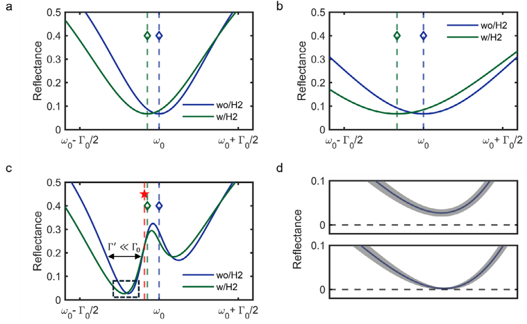
Plasmonic hydrogen sensors have enabled hydrogen detection below parts-per-million (ppm) range by boosting the sensitivity using localizedsurface plasmonic resonant (LSPR) structures. However, the intrinsic opticallosses of Palladium (Pd), the primary plasmonic metal used for hydrogen detection, result in a low quality (Q) factor LSPR, which fundamentally hinders further improvement. In this work, a hybrid plasmonic metasurface is proposed that couples Pd-based LSPR structure with an Au film supporting surface plasmon polariton mode (Au-SPP). The coupled near-perfect absorber resonance yields a spectrally narrow, high Q response that retains strong sensitivity to hydrogen while improving resonance localization. Numerical analysis shows that, under shot-noise-limited conditions, the limit of detection (LoD) can be improved by over threefold compared to the state-of-the-art designs. This hybrid plasmonic coupled-mode metasurface thus presents a promising pathway to achieve parts-per-billion-level (ppb-level) hydrogen detection with enhanced spectral precision and robustness.
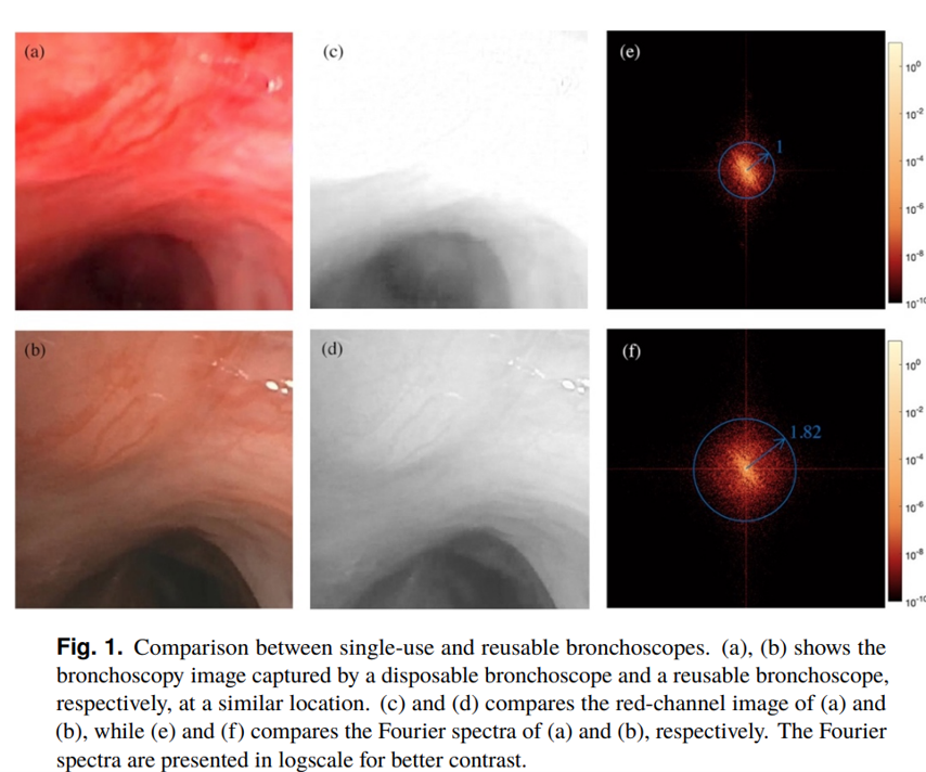
The COVID-19 pandemic underscored the need for safer and more cost-effective bronchoscopy solutions, leading to increased interest in single-use bronchoscopes due to their elimination of cross-contamination risk. However, their widespread adoption has been limited by inferior image quality compared to the reusable counterparts. Addressing this need, we present in this study a deep-learning framework specifically designed to enhance the imaging performance of single-use bronchoscopes, improving the signal-to-noise ratio and image resolution while maintaining real-time processing capability. Our approach integrates a generative adversarial network architecture with attention mechanisms that focus on airway assessment. We also introduce a combined loss function to close the quality gap between reusable and disposable bronchoscopes. Additionally, we propose Fourier spectra comparison as a performance metric to evaluate the neural network performance on improving real bronchoscopy videos in the absence of ground truth images. The neural network model was initially trained and evaluated on a simulated dataset, achieving an 89% improvement in PSNR and a 16% increase in SSIM. When applied to real bronchoscopy videos, the trained model demonstrated a 1.8-fold increase in resolution based on the Fourier-spectra metric. The reconstruction speed was also computed for images of varying sizes, confirming the network�s feasibility for real-time applications with large fields of view. This work not only presents a scalable AI solution that transforms disposable bronchoscopes into competitive alternatives for patients with respiratory disease but also establishes new methodological directions for evaluating and optimizing highly specialized medical imaging tasks in resource-constrained settings.
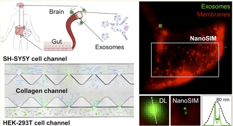
This study introduces an innovative nanophotonic biosensor system designed to explore exosome dynamics within the gut-brain axis, highlighting the bidirectional and biochemical communication between the gastrointestinal tract and the central nervous system. The proposed system incorporates coculture environments for various cell types, microfluidic control of exosomes, and super-resolution imaging capabilities for both exosomes and live cells. While enabling real-time observation of long-range exosome dynamics within the gut-brain-axis-on-a-chip, this approach offers superior spatial resolution for visualizing individual exosomes in both donor and recipient cells. Through precise microfluidic manipulation, exosomes are observed as they are secreted from donor cells, transported within the chip, and interact with recipient cells in a coculture environment, mimicking the communication process occurring in the gut-brain axis. The dynamics of exosome transport within the gut-brain axis model are expected to improve the understanding of their biological functions and potential applications.
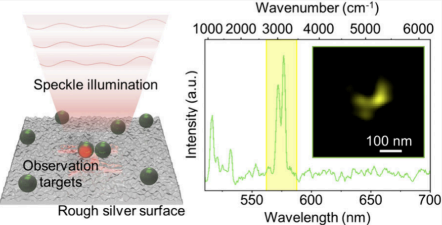
A super-resolution Raman scattering microscopy technique is demonstrated by combining localized surface plasmon-based structured illumination microscopy with the blindSIM algorithm. This approach enables super-resolution Raman scattering imaging of dielectric nanoparticles with sub-100 nm resolution. The technique leverages the surface-enhanced Raman scattering effect of rough silver films to generate near-field speckle patterns, enabling subdiffraction-limited optical sampling and enhanced Raman signals. The method demonstrates the excitation/emission modulation between emitters separated by subdiffraction distances. Experimental results reveal that background subtraction for Raman images from polystyrene beads generates image contrasts predominantly consisting of Raman-shifted photons. The enhanced signal-to-noise ratio obtained from 80 nm polystyrene beads proves sufficient for applying the blindSIM algorithm. The result presents a remarkable resolution enhancement, surpassing the diffraction limit by 4.4 times and successfully resolving 80 nm dielectric nanoparticles. This approach represents a significant advancement in label-free super-resolution imaging, offering potential applications in various fields of microscopy and materials science.
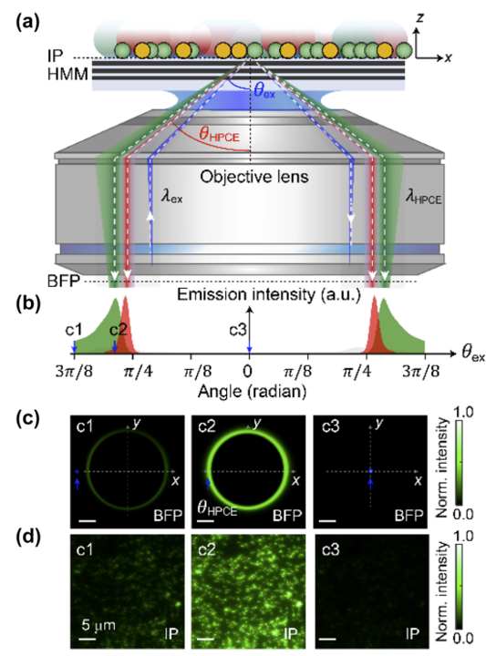
A new type of optical microscopy based on hyperbolic polariton-coupled emission (HPCE) is demonstrated. By employing hyperbolic metamaterials as the substrate, we show a nearly 6-fold increase in fluorescence intensity in the HPCE microscope compared to total internal reflection fluorescence (TIRF) on glass substrates. Moreover, we achieve precise, time-dependent control of the fluorescence intensity by modulating the incidence angle with a galvo scanner. This tunability offers extensive potential for applications in super-resolution fluorescence microscopy and highsensitivity sensing, enabling real-time fluorescence intensity adjustment.
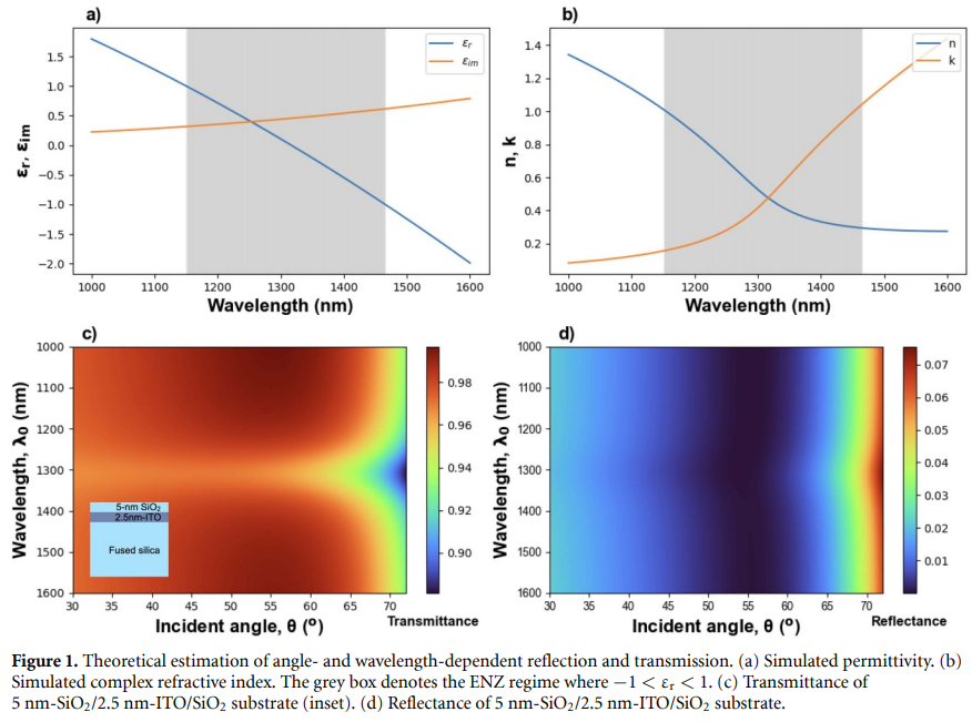
Due to its transparent and conductive nature, indium tin oxide (ITO) offers substantial benefits in several industries, such as thin film transistors, displays, and nanophotonics. Previous studies on ultrathin ITO have so far focused on its electrical properties but have neglected the technologically important epsilon-near-zero (ENZ) optical features due to the difficulty of extracting the refractive index and the thickness-dependent degradation of the optical properties. Here, we demonstrate a complementary metal-oxide-semiconductor (CMOS)-compatible deposition procedure for sub-percolation thickness (below 4 nm) ITO using a dry-etch assisted radiofrequency magnetron sputtering technique that yields continuous films in a precisely controlled manner. Through interface engineering and post-deposition annealing optimization, we show that these ITO films can retain high carrier mobility (43 cm2 V-1 s-1) while achieving a tunable near-zero-index (NZI) regime throughout the telecommunications band using a Berreman-assisted optical characterization technique. Our result opens the possibility of efficiently designing ENZ/NZI materials at the nanoscale using a robust fabrication approach for applications in nanophotonics
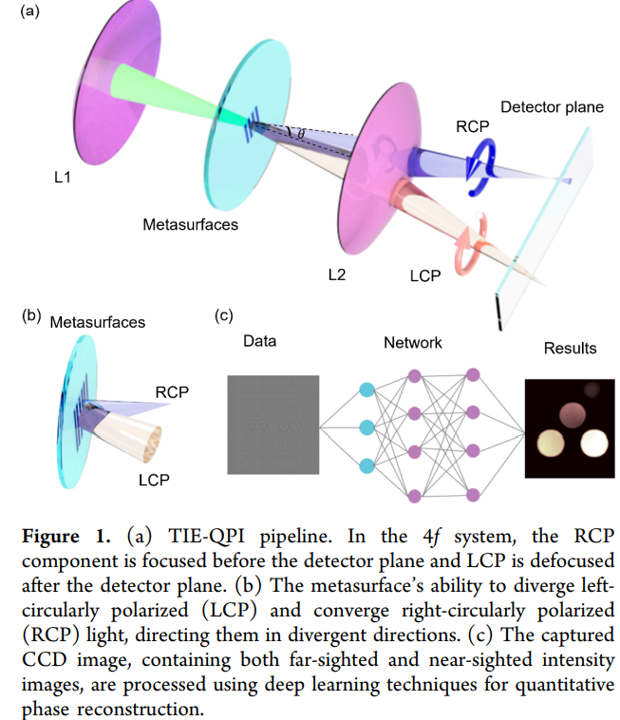
Quantitative optical phase information provides an alternative method to observe biomedical properties, where conventional phase imaging fails. Phase retrieval typically requires multiple intensity measurements and iterative computations to ensure uniqueness and robustness against detection noise. To increase the measurement speed, we propose a single-shot quantitative phase imaging method with metasurface optics that can be conveniently integrated into conventional imaging systems with minimal modification. The improvement of the measurement speed is simultaneously made possible by combining deep learning with the transport-ofintensity equation. As a proof-of-concept, we demonstrate phase retrieval on both calibrated phase objects and biological specimens by using an imaging system integrated with our metasurface. When combined with the matched neural network, the system yields result with errors as low as 5% and increased space-bandwidth-product. A multitude of commercial applications can benefit from the compactness and rapid implementation of our proposed method.
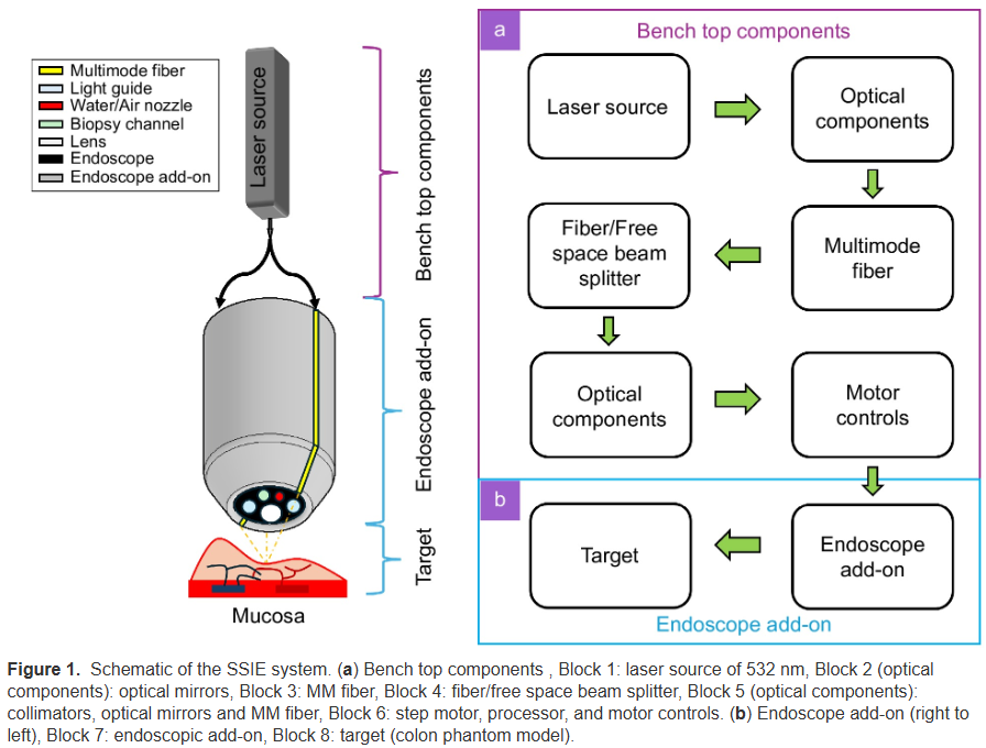
Structured illumination, a wide-field imaging approach used in microscopy to enhance image resolution beyond the system's diffraction limits, is a well-studied technique that has gained significant traction over the last two decades. However, when translated to endoscopic systems, severe deformations of illumination patterns occur due to the large depth of field (DOF) and the 3D nature of the targets, introducing significant implementation challenges. Hence, this study explores a speckle-based system that best suits endoscopic practices to enhance image resolution by using random illumination patterns. The study presents a prototypic model of an endoscopic add-on, its design, and fabrication facilitated by using the speckle structured illumination endoscopic (SSIE) system. The imaging results of the SSIE are explained on a colon phantom model at different imaging planes with a wide field of view (FOV) and DOF. The obtained imaging metrics are elucidated and compared with state-of-the-art (SOA) high-resolution endoscopic techniques. Moreover, the potential for a clinical translation of the prototypic SSIE model is also explored in this work. The incorporation of the add-on and its subsequent results on the colon phantom model could potentially pave the way for its successful integration and use in futuristic clinical endoscopic trials.
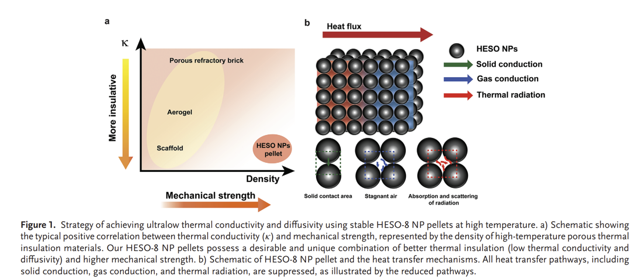
The realization of low thermal conductivity at high temperatures (0.11 W m-1 K-1 800 degC) in ambient air in a porous solid thermal insulation material, using stable packed nanoparticles of high-entropy spinel oxide with 8 cations (HESO-8 NPs) with a relatively high packing density of ~50%, is reported. The high-density HESO-8 NP pellets possess around 1000-fold lower thermal diffusivity than that of air, resulting in much slower heat propagation when subjected to a transient heat flux. The low thermal conductivity and diffusivity are realized by suppressing all three modes of heat transfer, namely solid conduction, gas conduction, and thermal radiation, via stable nanoconstriction and infrared-absorbing nature of the HESO-8 NPs, which are enabled by remarkable microstructural stability against coarsening at high temperatures due to the high entropy. This work can elucidate the design of the next-generation high-temperature thermal insulation materials using high-entropy ceramic nanostructures.
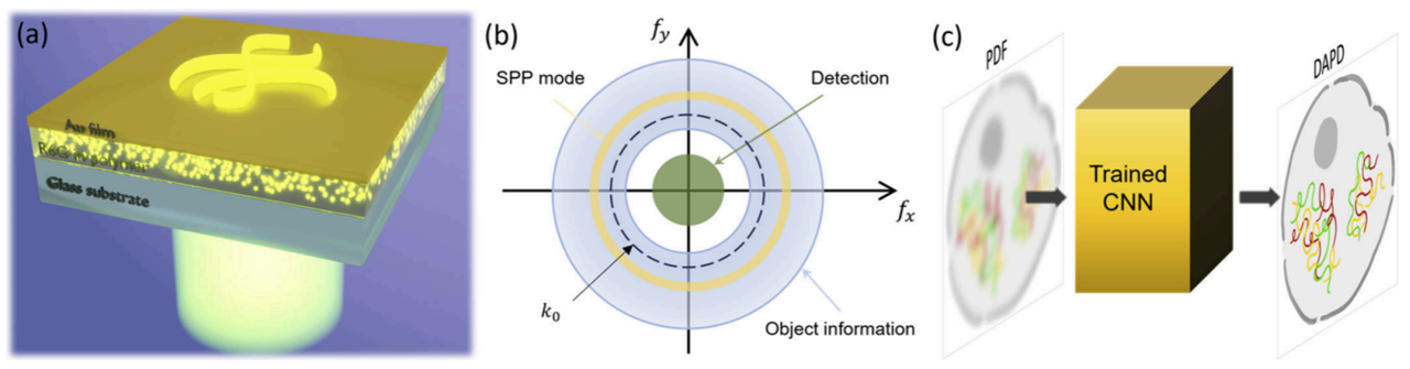
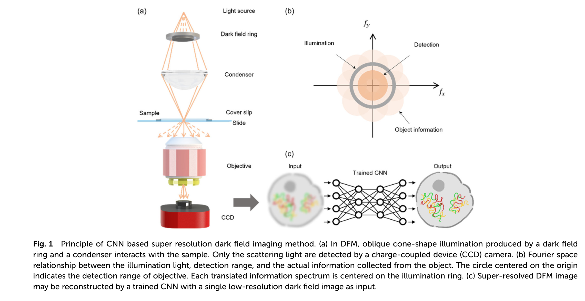
Dark-field microscopy (DFM) is a widely used imaging tool, due to its high-contrast capability in imaging labelfree specimens. Traditional DFM requires optical alignment to block the oblique illumination, and the resolution is diffraction-limited to the wavelength scale. In this work, we present deep-learning assisted plasmonic dark-field microscopy (DAPD), which is a single-frame super-resolution method using plasmonic dark-field (PDF) microscopy and deep-learning assisted image reconstruction. Specifically, we fabricated a designed PDF substrate with surface plasmon polaritons (SPPs) illuminating specimens on the substrate. Dark field images formed by scattered light from the specimen are further processed by a pretrained convolutional neural network (CNN) using a simulation dataset based on the designed substrate and parameters of the detection optics. We demonstrated a resolution enhancement of 2.8 times on various label-free objects with a large potential for future improvement. We highlight our technique as a compact alternative to traditional DFM with a significantly enhanced spatial resolution.
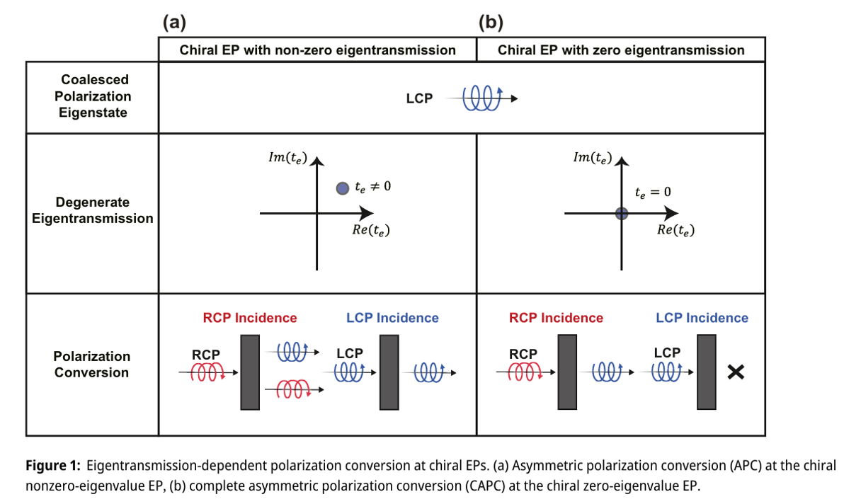
Non-Hermitian systems can be tuned to exhibit exceptional points, where both eigenvalues and eigenstates coalesce concurrently. The inherent adaptability of photonic non-Hermitian systems in configuring gain and loss has allowed us to observe a plethora of counterintuitive phenomena, largely as a consequence of the eigenspace reduction at these exceptional points. In this work, we propose a non-Hermitian metasurface that, through the incorporation of gain, enables complete asymmetric polarization conversion at an exceptional point with a zero eigenvalue. Specifically, we provide numerical evidence for this concept by designing a non-Hermitian metasurface that facilitates polarization conversion from right to left circular polarization, while preventing conversion in the reverse direction and co-polarized transmission. Furthermore, our investigation reveals that this specific form of complete asymmetric polarization conversion results in maximum circular dichroism in transmission, thereby eliminating the need for external chirality or three-dimensional helical structures. This non-Hermitian technique offers an intriguing approach to designing polarization-sensitive optical devices and systems, further expanding their functionalities and capabilities.
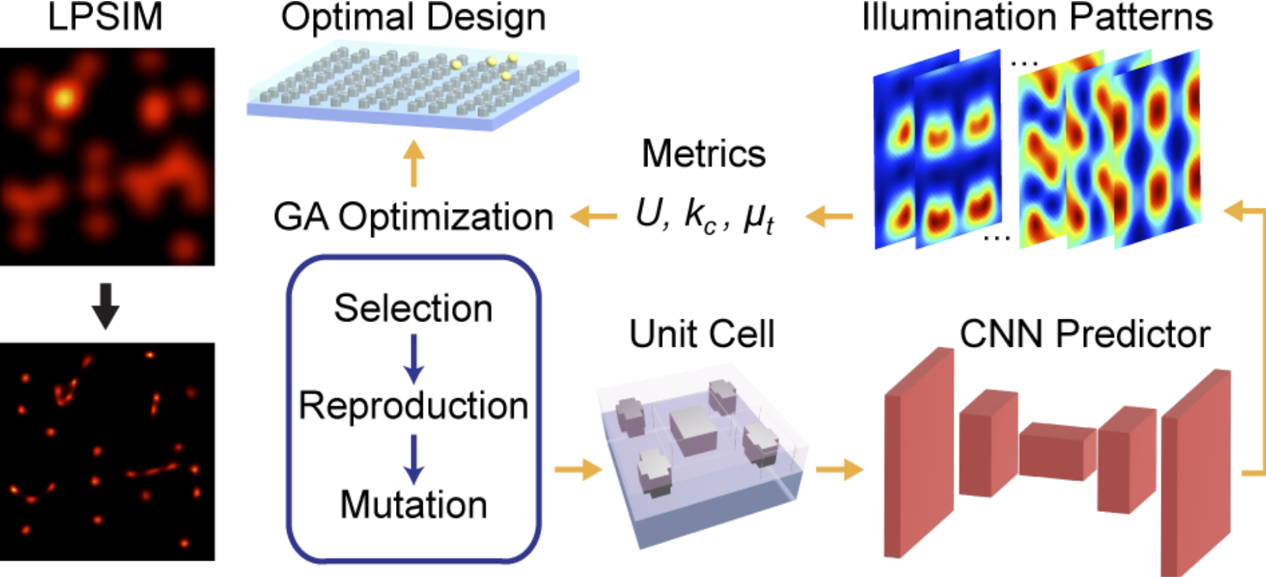
Super-resolution fluorescence imaging has offered unprecedented insights and revolutionized our understanding of biology. In particular, localized plasmonic structured illumination microscopy (LPSIM) achieves video-rate super-resolution imaging with ~50 nm spatial resolution by leveraging subdiffraction-limited nearfield patterns generated by plasmonic nanoantenna arrays. However, the conventional trial-and-error design process for LPSIM arrays is time-consuming and computationally intensive, limiting the exploration of optimal designs. Here, we propose a hybrid inverse design framework combining deep learning and genetic algorithms to refine LPSIM arrays. A population of designs is evaluated using a trained convolutional neural network, and a multiobjective optimization method optimizes them through iteration and evolution. Simulations demonstrate that the optimized LPSIM substrate surpasses traditional substrates, exhibiting higher reconstruction accuracy, robustness against noise, and increased tolerance for fewer measurements. This framework not only proves the efficacy of inverse design for tailoring LPSIM substrates but also opens avenues for exploring new plasmonic nanostructures in imaging applications.
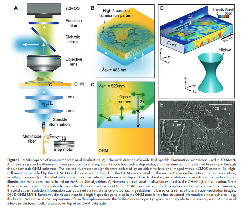
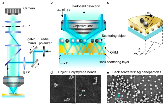
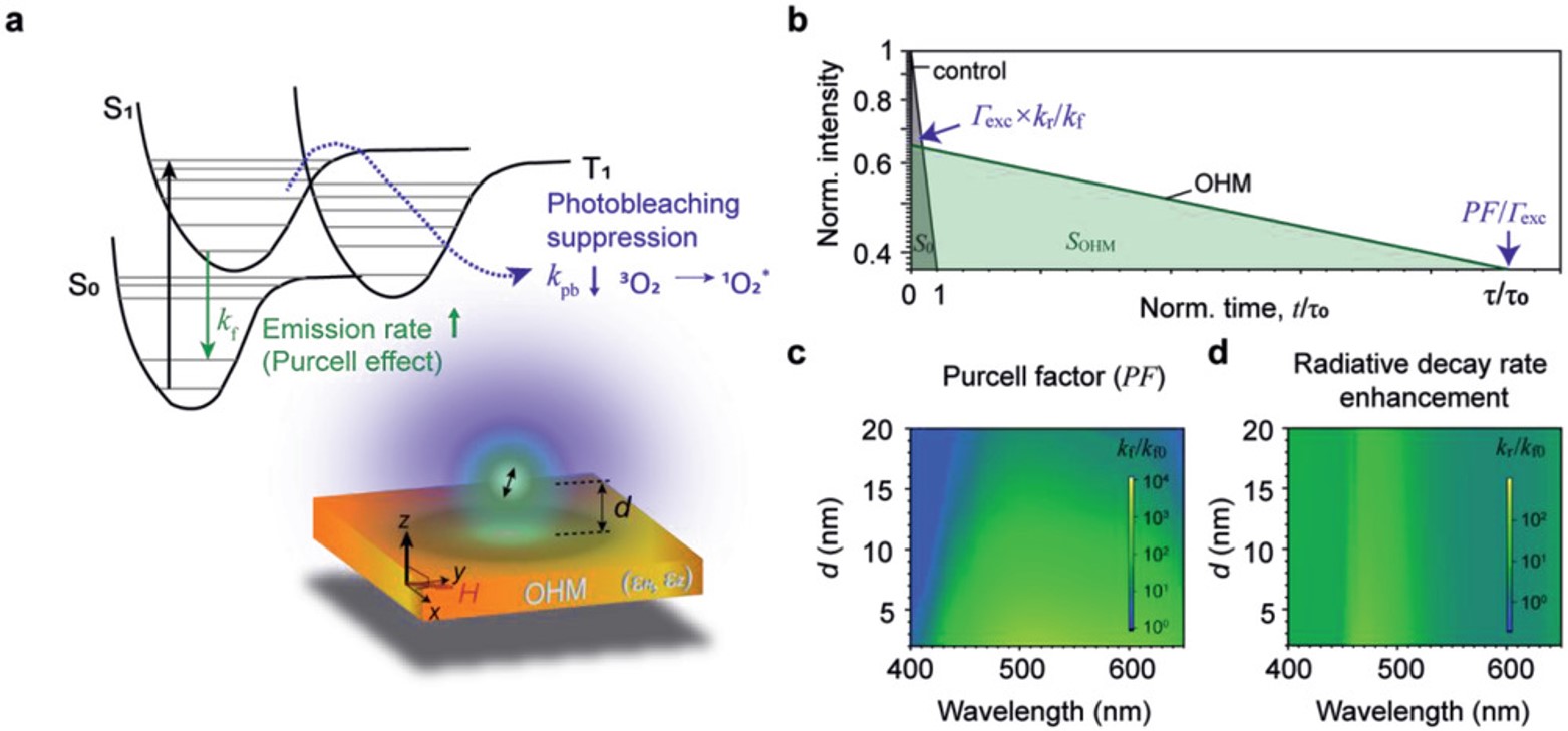
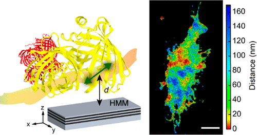
Recent advancements in optical metamaterials have opened new possibilities in the exciting field of super-resolution microscopies. The far-field metamaterial-assisted illumination nanoscopies (MAINs) have, very recently, enhanced the lateral resolution to one-fifteenth of the optical wavelength. However, the axial localization accuracy of fluorophores in the MAINs remains rarely explored. Here, a MAIN with a nanometer-scale axial localization accuracy is demonstrated by monitoring the distance-dependent photobleaching dynamics of the fluorophores on top of an organic hyperbolic metamaterial (OHM) substrate under a wide-field single-objective microscope. With such a regular experimental configuration, 3D imaging of various biological samples with the resolution of ~40 nm in the lateral dimensions and ~5 nm in the axial dimension is realized. The demonstrated imaging modality enables the resolution of the 3D morphology of nanoscopic cellular structures with a significantly simplified experimental setup.
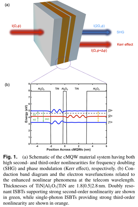
A material platform that excels in both optical secondand third-order nonlinearities at a telecom wavelength is theoretically and experimentally demonstrated. In this TiN-based coupled metallic quantum well structure, electronic subbands are engineered to support doubly resonant inter-subband transitions for an exceptionally high second-order nonlinearity and provide single-photon transitions for a remarkable third-order nonlinearity within the 1400�1600 nm bandwidth. The second-order susceptibility chi2 reaches 2840 pm/V at 1440 nm, while the Kerr coefficient n2 arrives at 2.8�10^-10 cm2/W at 1460 nm. The achievement of simultaneous strong second- and third-order nonlinearities in one material at a telecom wavelength creates opportunities for multi-functional advanced applications in the field of nonlinear optics
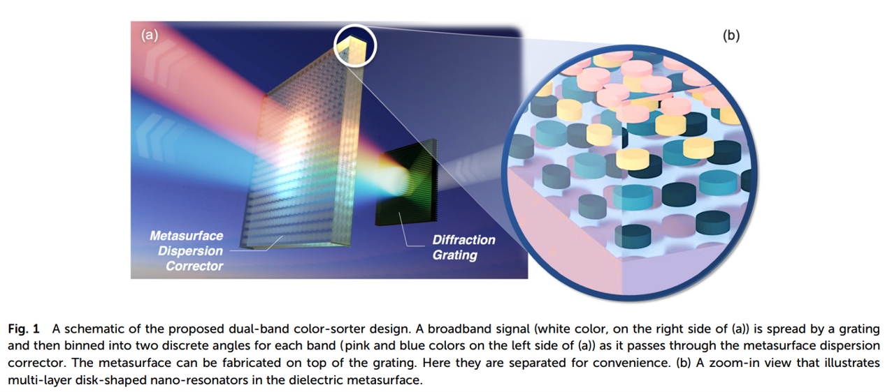
The process of sorting light based on colors (photon energy) is a prerequisite in broadband optical systems, typically achieved in the form of guiding incoming signals through a sequence of spectral filters. The assembly of filters often leads to lengthy optical trains and consequently, large system footprints. In this work, we address this issue by proposing a flat color-sorting device comprising a diffraction grating and a dielectric Huygens' metasurface. Upon the incidence of a broadband beam, the grating disperses wavelengths to a continuous range of angles in accordance with the law of diffraction. The following metasurface with multiple paired Huygens' resonances corrects the dispersion and binds wavelengths to the corresponding waveband with a designated output angle. We demonstrate the sorting efficacy by designing a device with a color-sorting metasurface with two discrete dispersion-compensated outputs (10.8 � 0.3 um and 11.9 � 0.3 um), based on the proposed approach. The optimized metasurface possesses an overall transmittance exceeding 57% and reduces lateral dispersion by 90% at the output. The proposed color-sorting mechanism provides a solution that benefits the designing of metasurfaces for miniature multi-band systems.
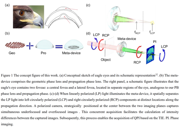
The dual-focus vision observed in eagles' eyes is an intriguing phenomenon that has long captivated scientists. Inspired by this natural occurrence, our research introduces a novel bifocal meta-device incorporating a polarized camera capable of simultaneously capturing images for two different polarizations with slightly different focal distances. This innovative approach facilitates the concurrent acquisition of underfocused and overfocused images in a single snapshot, enabling the effective extraction of quantitative phase information from the object using the transport of intensity equation. Experimental demonstrations showcase the application of quantitative phase imaging to artificial objects and human embryonic kidney cells, particularly emphasizing the meta-device's relevance in dynamic scenarios such as laser-induced ablation in human embryonic kidney cells. Moreover, it provides a solution for the quantification during the dynamic process at the cellular level. Notably, the proposed eagle-eye inspired meta-device for phase imaging (EIMPI), due to its simplicity and compact nature, holds promise for significant applications in fields such as endoscopy and headsets, where a lightweight and compact setup is essential.
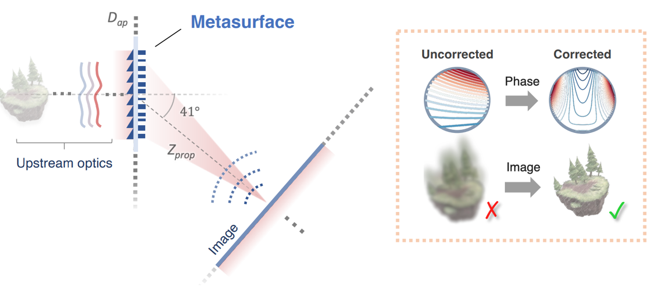
The rapid advancement of portable electronics has created enormous demand for compact optical imaging systems. Such systems often require folded optical systems with beam steering and shaping components to reduce sizes and minimize image aberration at the same time. In this study, we present a solution that utilizes an inverse-designed dielectric metasurface for arbitrary-angle image-relay with aberration correction. The metasurface phase response is optimized by a series of artificial neural networks to compensate for the severe aberrations in the deflected images and meet the requirements for device fabrication at the same time. We compare our results to the solutions found by the global optimization tool in Zemax OpticStudio and show that the proposed method can predict better point-spread functions and images with less distortion. Finally, we designed a metasurface to achieve the optimized phase profile.
Dark-field microscopy (DFM) is a powerful label-free and high-contrast imaging technique due to its ability to reveal features of transparent specimens with inhomogeneities. However, owing to the Abbe�s diffraction limit, fine structures at sub-wavelength scale are difficult to resolve. In this work, we report a single image super resolution DFM scheme using a convolutional neural network (CNN). A U-net based CNN is trained with a dataset which is numerically simulated based on the forward physical model of the DFM. The forward physical model described by the parameters of the imaging setup connects the object ground truths and dark field images. With the trained network, we demonstrate super resolution dark field imaging of various test samples with twice resolution improvement. Our technique illustrates a promising deep learning approach to double the resolution of DFM without any hardware modification.
Roadmap on Electromagnetic Metamaterials and Metasurfaces
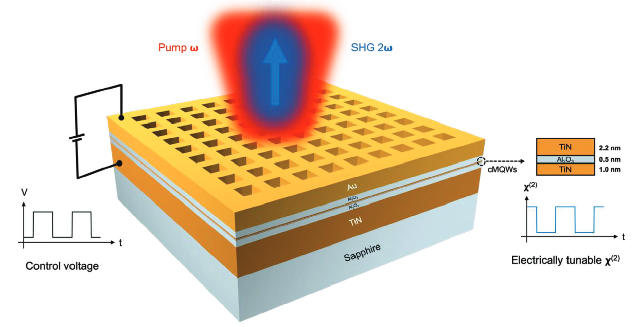
An electrically tunable nonlinear optical device working at near-infrared wavelength is theoretically and experimentally demonstrated. Ultrahigh optical second-order nonlinearity from titanium-nitride-based coupled metallic quantum wells can be electrically tuned by external electric field. Tunability of second-order susceptibility Χ2 reaches a 63% modulation depth with an average tunability of 10.5% per volt. In addition, electro-optic modulation of second-harmonic signal is presented by continuous tuning of Χ2 over a long period of time with high stability. These results provide a new material platform with actively controllable strong nonlinearity for future nonlinear photonic systems, such as ultra-compact opto-electronic modulation devices and reconfigurable nonlinear metamaterials and metasurfaces.
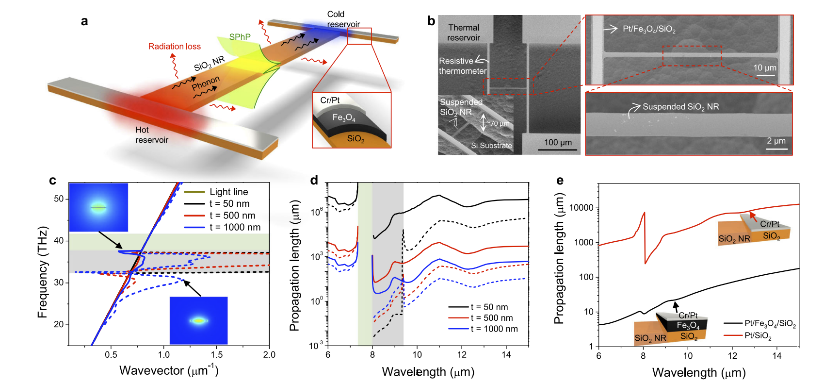
Heat conduction in solids is typically governed by the Fourier�s law describing a diffusion process due to the short wavelength and mean free path for phonons and electrons. Surface phonon polaritons couple thermal photons and optical phonons at the surface of polar dielectrics, possessing much longer wavelength and propagation length, representing an excellent candidate to support extraordinary heat transfer. Here, we realize clear observation of thermal conductivity mediated by surface phonon polaritons in SiO2 nanoribbon waveguides of 20-50 nm thick and 1-10 um wide and also show nonFourier behavior in over 50-100 um distance at room and high temperature. This is enabled by rational design of the waveguide to control the mode size of the surface phonon polaritons and its efficient coupling to thermal reservoirs. Our work laid the foundation for manipulating heat conduction beyond the traditional limit via surface phonon polaritons waves in solids.
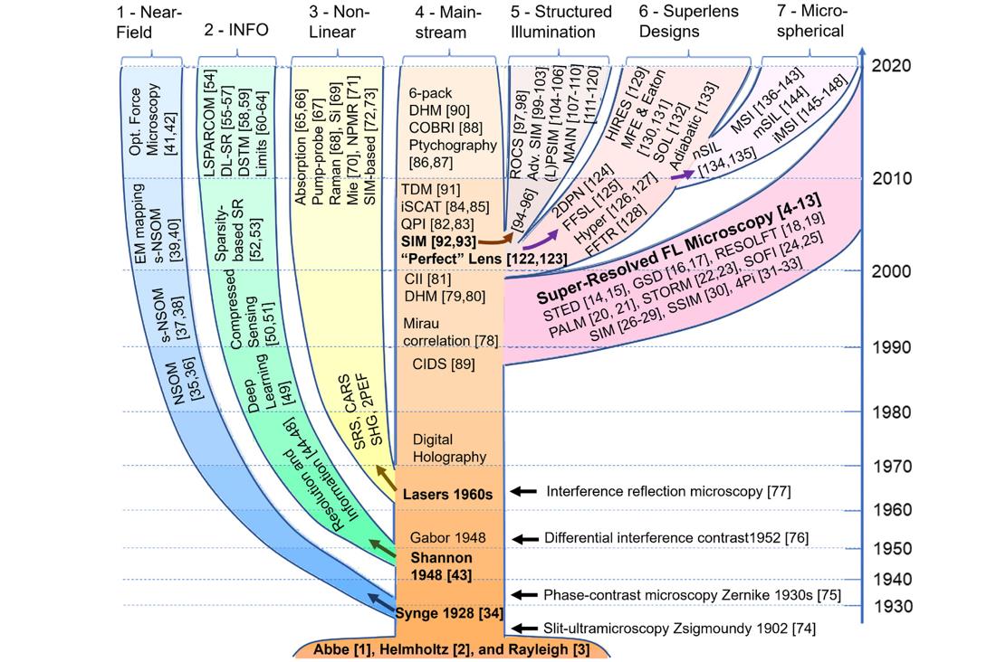
Label-free super-resolution (LFSR) imaging relies on light-scattering processes in nanoscale objects without a need for fluorescent (FL) staining required in super-resolved FL microscopy. The objectives of this Roadmap are to present a comprehensive vision of the developments, the state-of-the-art in this field, and to discuss the resolution boundaries and hurdles that need to be overcome to break the classical diffraction limit of the label-free imaging. The scope of this Roadmap spans from the advanced interference detection techniques, where the diffraction-limited lateral resolution is combined with unsurpassed axial and temporal resolution, to techniques with true lateral super-resolution capability that are based on understanding resolution as an information science problem, on using novel structured illumination, near-field scanning, and nonlinear optics approaches, and on designing superlenses based on nanoplasmonics, metamaterials, transformation optics, and microsphere-assisted approaches. To this end, this Roadmap brings under the same umbrella researchers from the physics and biomedical optics communities in which such studies have often been developing separately. The ultimate intent of this paper is to create a vision for the current and future developments of LFSR imaging based on its physical mechanisms and to create a great opening for the series of articles in this field.
Quantitative amplitude and phase imaging (QAPI) has been an effective technique to examine label-free biomedical samples. Simple and reliable QAPI techniques realized by replacing conventional bulky optical elements with planar structures will improve the system portability and facilitate in vivo imaging applications. Here, we propose a single-shot QAPI method realized by simply inserting a pair of all-dielectric geometric phase metasurfaces into a traditional microscope. The first metasurface splits a linearly polarized incident beam into two circularly polarized components and the following metasurface deflects the two beams back toward their initial directions. The metasurface pair generates two laterally displaced replicas of the input object, of which the interference forms a retardance image with a bias retardation controlled by an analyzer. The amplitude and phase information of the object is reconstructed from four retardance images simultaneously recorded by a polarized camera. The metasurface pair can be placed near any conjugate plane of the object, which provides a flexible and robust configuration for QAPI, demonstrating its wide usage in live imaging.
Structured illumination microscopy (SIM) is one of the most widely applied wide field super resolution imaging techniques with high temporal resolution and low phototoxicity. The spatial resolution of SIM is typically limited to two times of the diffraction limit and the depth of field is small. In this work, we propose and experimentally demonstrate a low cost, easy to implement, novel technique called speckle structured illumination endoscopy (SSIE) to enhance the resolution of a wide field endoscope with large depth of field. Here, speckle patterns are used to excite objects on the sample which is then followed by a blind-SIM algorithm for super resolution image reconstruction. Our approach is insensitive to the 3D morphology of the specimen, or the deformation of illuminations used. It greatly simplifies the experimental setup as there are no calibration protocols and no stringent control of illumination patterns nor focusing optics. We demonstrate that the SSIE can enhance the resolution 2�4.5 times that of a standard white light endoscopic (WLE) system. The SSIE presents a unique route to super resolution in endoscopic imaging at wide field of view and depth of field, which might be beneficial to the practice of clinical endoscopy.

Recent progress in the Valley Hall insulator has demonstrated a nontrivial topology property due to the distinct valley index in 2D semiconductor systems. In this work, we propose a highly tunable topological phase transition based on valley photonic crystals. The topological phase transition is realized by the inversion symmetry broken due to the refractive index change of structures consisting of optical phase change material (OPCM) with thermal excitation of different sites in a honeycomb lattice structure. Besides, simulations of light propagation at sharp corners and pseudo-spin photon coupling are conducted to quantitatively examine the topological protection. Compared with other electro-optical materials based on reconfigurable topological photonics, a wider bandwidth and greater tunability of both central bandgap frequency and topological phase transition can happen in the proposed scheme. Our platform has great potential in practical applications in lasing, light sensing, and high-contrast tunable optical filters.
The dielectric metasurface has become a powerful tool for compact optical components with various wavefront controlling functionalities accompanied by negligible losses at the corresponding working frequencies. In this work, we propose a tunable all-dielectric metasurface as an optical filter with high resolution covering different optical communication bands, where tunability is realized by a combination of changing the incident angle and modulating the refractive index of an optical phase changing material (OPCM). When the incident angle varies, our optical filter based on a two-dimensional bound state in continuums (BIC) metasurface can achieve sequential, extremely sharp resonances. In addition, the resonance peaks could be further shifted to a different frequency band by the refractive index change of OPCM via pulsed laser heating. The proposed scheme can offer optical filters with high spectral resolution and large tunable working wavelength range, which greatly benefits from the topological property of BIC and large modulation depth of OPCM.
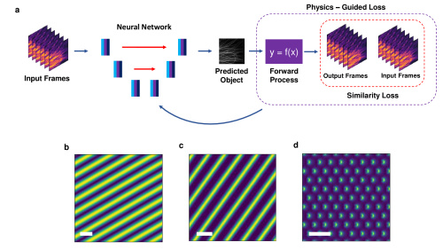
Structured illumination microscopy (SIM) is a popular super-resolution imaging technique that can achieve resolution improvements of 2� and greater depending on the illumination patterns used. Traditionally, images are reconstructed using the linear SIM reconstruction algorithm. However, this algorithm has hand-tuned parameters which can often lead to artifacts, and it cannot be used with more complex illumination patterns. Recently, deep neural networks have been used for SIM reconstruction, yet they require training sets that are difficult to capture experimentally. We demonstrate that we can combine a deep neural network with the forward model of the structured illumination process to reconstruct sub-diffraction images without training data. The resulting physics-informed neural network (PINN) can be optimized on a single set of diffraction-limited sub-images and thus does not require any training set. We show, with simulated and experimental data, that this PINN can be applied to a wide variety of SIM illumination methods by simply changing the known illumination patterns used in the loss function and can achieve resolution improvements that match theoretical expectations.
Fluorescence super-resolution microscopy has, over the last two decades, been extensively developed to access deep-subwavelength nanoscales optically. Label-free super-resolution technologies however have only achieved a slight improvement compared to the diffraction limit. In this context, we demonstrate a label-free imaging method, i.e., hyperbolic material enhanced scattering (HMES) nanoscopy, which breaks the diffraction limit by tailoring the light-matter interaction between the specimens and a hyperbolic material substrate. By exciting the highly confined evanescent hyperbolic polariton modes with dark-field detection, HMES nanoscopy successfully shows a high-contrast scattering image with a spatial resolution around 80 nm. Considering the wavelength at 532 nm and detection optics with a 0.6 numerical aperture (NA) objective lens, this value represents a 5.5-fold resolution improvement beyond the diffraction limit. HMES provides capabilities for super-resolution imaging where fluorescence is not available or challenging to apply.
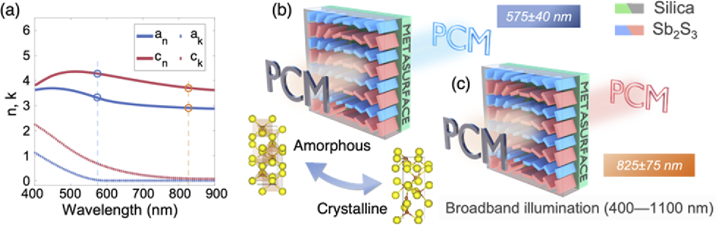
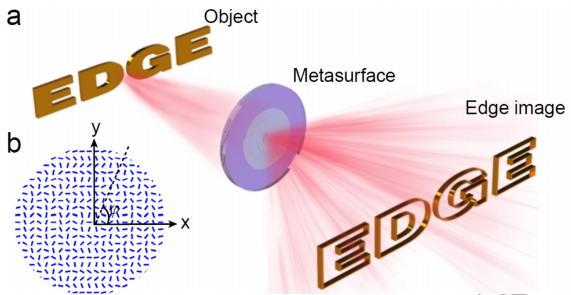
Optical edge detection at the visible and near infrared (VNIR) wavelengths is deployed widely in many areas. Here we demonstrate numerically transmissive VNIR dual band edge imaging with a switchable metasurface. Tunability is enabled by using a low-loss and reversible phase-change material Sb2S3. The metasurface acts simultaneously as a high-pass spatial filter and a tunable spectral filter, giving the system the freedom to switch between two functions. In Function 1 with amorphous Sb2S3, this metasurface operates in the edge detection mode near 575 nm and blocks near infrared (NIR) transmission. In Function 2 with crystalline Sb2S3, the device images edges near 825 nm and blocks visible light images. The switchable Sb2S3 metasurfaces allow low cross talk edge imaging of a target without complicated optomechanics.
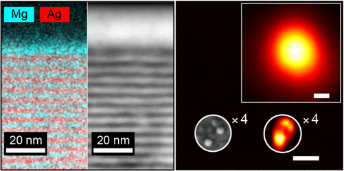
Metamaterial-assisted illumination nanoscopy (MAIN) has been proven to be a promising approach for super-resolution microscopy with up to a 7-fold improvement in imaging resolution. Further resolution enhancement is possible in principle, however, has not yet been demonstrated due to the lack of high-quality ultrathin layered hyperbolic metamaterials (HMMs) used in the MAIN. Here, we fabricate a low-loss composite HMM consisting of high-quality bilayers of Al-doped Ag and MgO with a nominal thickness of 2.5 nm, and then use it to demonstrate an ultrathin layered hyperbolic metamaterial-assisted illumination nanoscopy (ULH-MAIN) with a 14-fold imaging resolution improvement. This improvement of resolution is achieved in fluorescent beads super-resolution experiments and verified with scanning electron microscopy. The ULH-MAIN presents a simple super-resolution imaging approach that offers distinct benefits such as low illumination power, low cost, and a broad spectrum of selectable probes, making it ideal for dynamic imaging of life science samples.
In this Letter, we propose a new quantitative phase imaging methodology named Fourier optical spin splitting microscopy (FOSSM). FOSSM relies on a metasurface located at the Fourier plane of a polarized microscope to separate the object image into two replicas of opposite circularly polarized states. The bias retardation between the two replicas is tuned by translating the metasurface or rotating the analyzer. Combined with a polarized camera, FOSSM can easily achieve single-shot quantitative phase gradient imaging, which greatly reduces the complexity of current phase microscope setups, paving the way for the next generation high-speed real-time multifunctional microscopy.
Optical image processing and computing systems provide supreme information processing rates by utilizing parallel optical architectures. Existing optical analog processing techniques require multiple devices for projecting images and executing computations. In addition, those devices are typically limited to linear operations due to the time-invariant optical responses of the building materials. In this work, a single metalens with an illumination intensity dependent coherent transfer function (CTF) is proposed and experimentally demonstrated, which performs varying computed imaging without requiring any additional optical components. The metalens consisting of nanoantenna structures with a static geometric phase and a nonlinear metallic quantum well layer offering an intensity-dependent dynamic phase results in a continuously tunable CTF. The approach allows for a weighted summation of two designed functions based on the metalens design, which potentially enables all optical computations of complex functions. The nonlinear metalens may lead to important applications in optical neural networks and parallel analog computing.
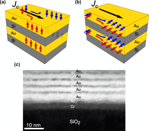
Investigation of the spin Hall effect in gold has triggered increasing interest over the past decade, since gold combines the properties of a large bulk spin-diffusion length and strong interfacial spin-orbit coupling. However, discrepancies between the values of the spin Hall angle of gold reported in the literature have brought into question the microscopic origin of the spin Hall effect in Au. Here, we investigate the thickness dependence of the effective spin-charge conversion efficiency in single Au films and ultrathin Au/Si multilayers by nonlocal transport and spin-torque ferromagnetic resonance measurements. We show that the inferred effective spin-charge conversion efficiency is strongly enhanced in ultrathin Au/Si multilayers, reaching exceedingly large values of 0.99 � 0.34 when the thickness of the individual Au layers is scaled down to 2 nm. These findings reveal the coexistence of a strong interfacial spin-to-charge conversion effect, which becomes dominant in ultrathin Au, and bulk spin Hall effect with a relatively low bulk spin Hall angle of 0.012 � 0.005. Our experimental results suggest the key role of the intrinsic spin Hall effect enhancement along with a strong interfacial spin-orbit coupling-related effect in the large spin-to-charge conversion in ultrathin Au.
Resolution capability of the linear structured illumination microscopy (SIM) plays a key role in its applications in physics, medicine, biology, and life science. Many advanced methodologies have been developed to extend the resolution of structured illumination by using subdiffraction-limited optical excitation patterns. However, obtaining SIM images with a resolution beyond 40 nm at visible frequency remains as an insurmountable obstacle due to the intrinsic limitation of spatial frequency bandwidth of the involved materials and the complexity of the illumination system. Here, a low-loss natural organic hyperbolic material (OHM) that can support record high spatial-frequency modes beyond 50k0, i.e., effective refractive index larger than 50, at visible frequencies is reported. OHM-based speckle structured illumination microscopy demonstrates imaging resolution at 30 nm scales with enhanced fluorophore photostability, biocompatibility, easy to use and low cost. This study will open up a new route in super-resolution microscopy by utilizing OHM films for various applications including bioimaging and sensing.
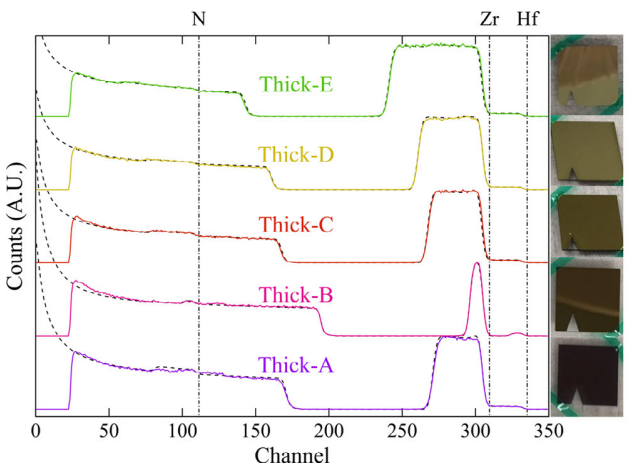
Recently, the application of transition metal mononitrides (TMNs) to plasmonics and nonlinear optics has grown at an astounding rate. TiN and ZrN have emerged as the dominating materials in this direction. However, even though ZrN is reported to have lower dielectric losses and enhanced tunability in plasmonic applications when compared with TiN, the body of work regarding TiN is much more mature than that of ZrN. This imbalance of work regarding ZrN may be in part an effect of pollution in precursor materials for the fabrication of ZrN, leading to an increased imaginary part of permittivity and frustration in reproduction of ZrN with literature-like properties. Herein, the effects of Hf defects (a common pollutant in Zr) on the optical properties of nitride films grown with radio frequency (RF) magnetron sputtering are reported. Hf defects are introduced into nitride films with a sputtering target made of the Hf-polluted "grade 702" Zr alloy. Hf defects are found in all analyzed films with concentrations at around ≈0.5-1 at %. Chemical, structural, and optical properties of RF magnetron-sputtered Hfx:Zry Nz films (x≫y,z) are characterized and discussed.
Within the last decade, genetic engineering and synthetic biology have revolutionized society�s ability to mass-produce complex biological products within genetically-modified microorganisms containing elegantly designed genetic circuitry. However, many challenges still exist in developing bioproduction processes involving genetically modified microorganisms with complex or multiple gene circuits. These challenges include the development of external gene expression regulation methods with the following characteristics: spatial�temporal control and scalability, while inducing minimal permanent or irreversible system-wide conditions. Different stimuli have been used to control gene expression and mitigate these challenges, and they can be characterized by the effect they produce in the culture media conditions. Invasive stimuli that cause permanent, irreversible changes (pH and chemical inducers), non-invasive stimuli that cause partially reversible changes (temperature), and non-invasive stimuli that cause reversible changes in the media conditions (ultrasound, magnetic fields, and light).

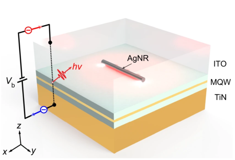
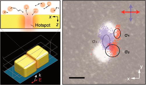
On-chip plasmonic circuitry offers a promising route to meet the ever-increasing requirement for device density and data bandwidth in information processing. As the key building block, electrically-driven nanoscale plasmonic sources such as nanoLEDs, nanolasers, and nanojunctions have attracted intense interest in recent years. Among them, surface plasmon (SP) sources based on inelastic electron tunneling (IET) have been demonstrated as an appealing candidate owing to the ultrafast quantum-mechanical tunneling response and great tunability. However, the major barrier to the demonstrated IET based SP sources is their low SP excitation efficiency due to the fact that elastic tunneling of electrons is much more efficient than inelastic tunneling. Here, we remove this barrier by introducing resonant inelastic electron tunneling (RIET)�follow a recent theoretical proposal�at the visible/near-infrared (NIR) frequencies and demonstrate highly efficient electrically driven SP sources. In our system, RIET is supported by a TiN/Al2O3 metallic quantum well (MQW) heterostructure, while monocrystalline silver nanorods (AgNRs) were used for the SP generation (localized surface plasmons (LSPs)). In principle, this RIET approach can push the external quantum efficiency (EQE) close to unity, opening up a new era of SP sources for not only high-performance plasmonic circuitry, but also advanced optical sensing applications.
Structured illumination microscopy (SIM) is one of the most powerful and versatile optical super- resolution techniques. Compared with other super-resolution methods, SIM has shown its unique advantages in wide-field imaging with high temporal resolution and low photon damage. However, traditional SIM only has about 2 times spatial resolution improvement compared to the diffraction limit. In this work, we propose and experimentally demonstrate an easily-implemented, low-cost method to extend the resolution of SIM, named speckle metamaterial-assisted illumination nanoscopy (speckle-MAIN). A metamaterial structure is introduced to generate speckle-like sub-diffraction-limit illumination patterns in the near field with improved spatial frequency. Such patterns, similar to traditional SIM, are then used to excite objects on top of the surface. We demonstrate that speckle-MAIN can bring the resolution down to 40 nm and beyond. Speckle-MAIN represents a new route for super-resolution, which may lead to important applications in bio-imaging and surface characterization.
Determining the axial position of an emitter with nanoscale precision is critical to a fundamental imaging methodology. While there are many advanced optical techniques being applied to high-resolution imaging, high-axial-resolution topography imaging of living cells is particularly challenging. Here, we present an application of metamaterial-assisted photobleaching microscopy (MAPM) with high-axial resolution to characterize morphological properties of living cells. Quantitative imaging of changes in the morphology of live cells is obtained by topographic and statistical analysis. The time-lapse topography image using the metamaterial-induced photostability provides information about growth factor induced changes in the cell morphology with high-axial resolution.
The dynamics of photons in fluorescent molecules plays a key role in fluorescence imaging, optical sensing, organic photovoltaics, and displays. Photobleaching is an irreversible photodegradation process of fluorophores, representing a fundamental limitation in relevant optical applications. Chemical reagents are used to suppress the photobleaching rate but with exceptionally high specificity for each type of fluorophore. Here, using organic hyperbolic materials (OHMs), an optical platform to achieve unprecedented fluorophore photostability without any chemical specificity is demonstrated. A more than 500-fold lengthening of the photobleaching lifetime and a 230-fold increase in the total emitted photon counts are observed simultaneously. These exceptional improvements solely come from the low-loss hyperbolic dispersion of OHM films and the large resultant Purcell effect in the visible spectral range. The demonstrated OHM platform may open up a new paradigm in nanophotonics and organic plasmonics for super-resolution imaging and the engineering of light-matter interactions at the nanoscale.
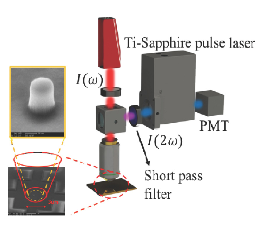
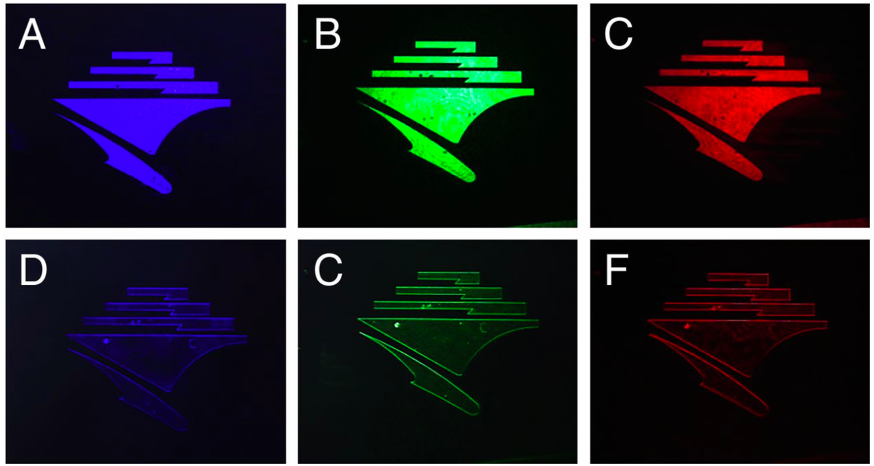
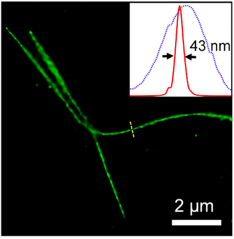
We report the second-harmonic generation (SHG) from single GaN nanowire. The diameter of the GaN nanowire varies from 150 to 400 nm. We present a model for the SHG process in the GaN nanowire; the analysis shows quantitatively that the SHG is dominated by its surface area. The effective second order nonlinear optical susceptibility (χ(2)eff) increases as the diameter of the GaN nanowire decreases. For 150-nm diameter GaN nanowire, χ(2)eff reaches 136 pm/V.
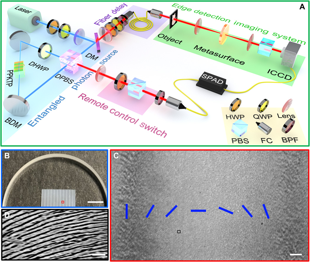
Metasurfaces consisting of engineered dielectric or metallic structures provide unique solutions to realize exotic phenomena including negative refraction, achromatic focusing, electromagnetic cloaking, and so on. The intersection of metasurface and quantum optics may lead to new opportunities but is much less explored. Here, we propose and experimentally demonstrate that a polarization-entangled photon source can be used to switch ON or OFF the optical edge detection mode in an imaging system based on a high-efficiency dielectric metasurface. This experiment enriches both fields of metasurface and quantum optics, representing a promising direction toward quantum edge detection and image processing with remarkable signal-to-noise ratio.
Optical metasurfaces have emerged as promising candidates for multifunctional devices. Dynamically reconfigurable metasurfaces have been introduced by employing phase-change materials or by applying voltage, heat, or strain. While existing metasurfaces exhibit appealing properties, they do not express any significant nonlinear effects due to the negligible nonlinear responses from the typical materials used to build the metasurface. In this work, we propose and experimentally demonstrate one kind of Kerr metasurface that shows strong intensity-dependent responses. The Kerr metasurface is composed of a top layer of gold antennas, a dielectric spacer, and a ground layer of metallic quantum wells (MQWs). Because of the large Kerr nonlinearity supported by the MQWs, the effective optical properties of the MQWs can change from metallic to dielectric with increasing of the input intensity, leading to dramatic modifications of the metasurface responses. This opens up new routes for potential applications in the field of nonlinear optics.
Optical analog signal processing technology has been widely studied and applied in a variety of science and engineering fields. It overcomes low-speed and high-power consumption disadvantages compared with its digital counterparts. Meanwhile, the emerging metasurface technology has been introduced to optical imaging and processing system and attracted much attentions. Here, we demonstrate the first broadband two-dimensional spatial differentiation and high-contrast edge imaging based on a dielectric metasurface across the whole visible spectrum. This edge detection method works for both intensity and phase objects simply by inserting the metasurface into a commercial optical microscope. The exploration of the highly efficient metasurface performing a basic optical differentiation operation opens new opportunities in applications of fast, compactible and power-efficient ultrathin devices for data processing and biological imaging.
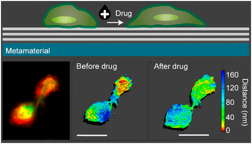
The past two decades have witnessed a dramatic progress in the development of novel super-resolution fluorescence microscopy technologies. Here, we report a new fluorescence imaging method, called metamaterial-assisted photobleaching microscopy (MAPM), which possesses a nanometer-scale axial resolution and is suitable for broadband operation across the entire visible spectrum. The photobleaching kinetics of fluorophores can be greatly modified via a separation-dependent energy transfer process to a nearby metamaterial. The corresponding photobleaching rate is thus linked to the distance between the fluorophores and the metamaterial layer, leading to a reconstructed image with exceptionally high axial resolution. We apply the MAPM technology to image the HeLa cell membranes tagged with fluorescent proteins and demonstrate an axial resolution of ~2.4 nm with multiple colors. MAPM utilizes a metamaterial-coated substrate to achieve super-resolution without altering anything else in a conventional microscope, representing a simple solution for fluorescence imaging at nanometer axial resolution.
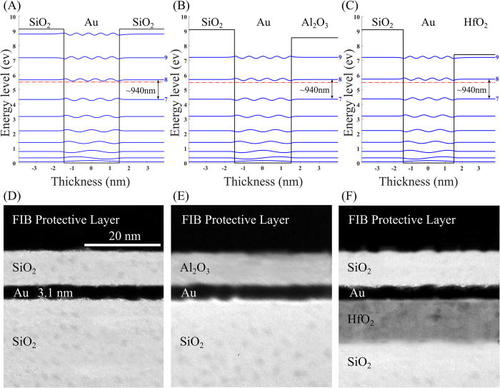
Investigation of new plasmonic material platforms with large optical nonlinearity is crucial for the continued development of nonlinear optics and its applications. Here, we report an enhanced second-order nonlinear effect in metallic quantum wells (QWs), where the intersubband transition plays a dominant role. Centrosymmetry in these metallic QWs is broken by forming multilayers with chemically and structurally distinct barrier oxides above and below a metal nanofilm. For Au-based QWs, we show that a large χ(2) around 229.6 pm/V in the near infrared was achieved in an asymmetric metallic QW of SiO2/Au/HfO2 on a fused silica substrate.
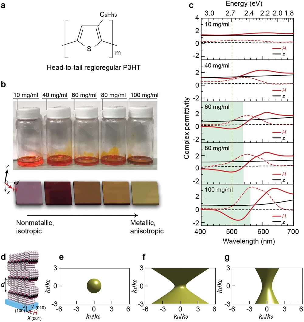
Hyperbolic media strengthen numerous attractive applications in optics such as super-resolution imaging, enhanced spontaneous emission, and nanoscale waveguiding. Natural hyperbolic materials exist at visible frequencies; however, implementations of these materials suffer substantial compromises resulting from the high loss in the currently available candidates. Here, the first experimental and theoretical investigation of regioregular poly(3-alkylthiophenes) (rr-P3ATs), a naturally low-loss organic hyperbolic material (OHM) in the visible frequency range, is shown. These hyperbolic properties arise from a highly ordered structure of layered electron-rich conjugated thiophene ring backbones separated by insulating alkyl side chains. The optical and electronic properties of the rr-P3AT can be tuned by controlling the degree of crystallinity and alkyl side chain length. First-principles calculations support the experimental observations, which result from the rr-P3AT's structural and optical anisotropy. Conveniently, rr-P3AT-based OHMs are facile to fabricate, flexible, and biocompatible, which may lead to tremendous new opportunities in a wide range of applications.
The strongly enhanced and confined subwavelength optical fields near plasmonic nanoantennas have been extensively studied not only for the fundamental understanding of light�matter interactions at the nanoscale but also for their emerging practical application in enhanced second harmonic generation, improved inelastic electron tunneling, harvesting solar energy, and photocatalysis. However, owing to the deep subwavelength nature of plasmonic field confinement, conventional optical imaging techniques are incapable of characterizing the optical performance of these plasmonic nanoantennas. Here, we demonstrate super-resolution imaging of ~20 nm optical field confinement by monitoring randomly moving dye molecules near plasmonic nanoantennas. This Brownian optical microscopy is especially suitable for plasmonic field characterization because of its capabilities for polarization sensitive wide-field super-resolution imaging.
The past several decades have witnessed rapid development of high-intensity, ultrashort pulse lasers, enabling deeper laboratory investigation of nonlinear optics, plasma physics, and quantum science and technology than previously possible. Naturally, with their increasing use, the risk of accidental damage to optical detection systems rises commensurately. Thus, various optical limiting mechanisms and devices have been proposed. However, restricted by the weak optical nonlinearity of natural materials, state-of-the-art optical limiters rely on bulk liquid or solid media, operating in the transmission mode. Device miniaturization becomes complicated with these designs while maintaining superior integrability and controllability. Here, we demonstrate a reflection-mode pulse limiter (sub�100 nm) using nanoscale refractory films made of Al2O3/TiN/Al2O3 metallic quantum wells (MQWs), which provide large and ultrafast Kerr-type optical nonlinearities due to the quantum size effect of the MQW. Functional multilayers consisting of these MQWs could find important applications in nanophotonics, nonlinear optics, and meta-optics.
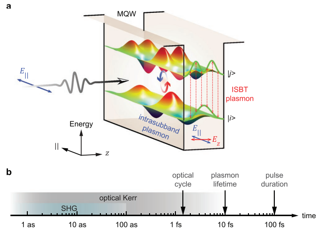
Intersubband transitions (ISBTs) in conduction and quantum wells (QWs) have attracted tremendous attention for their high technological potential, ranging from quantum cascade lasers, quantum well infrared photodetectors, to various nonlinear optical elements. One of the main characteristics of using the ISBTs is their polarization selection rule, which forbids a normal ncidence geometry. Here, it is shown that the ISBT selection rule is not strict on optical nonlinearities in metallic QWs (MQWs). The nonlinear process of second harmonic generation nearly follows the selection rule, while the optical Kerr nonlinear process severely deviates from it. The anomalous optical selection rules result from the non egligible ultrafast electron lectron scattering in these plasmonic systems, and a coupled mode theory is provided to get a physical grasp of the problem. The flexible selection rule in MQWs could bring drastic improvements in efficiency and diversity of ISBT ased devices.
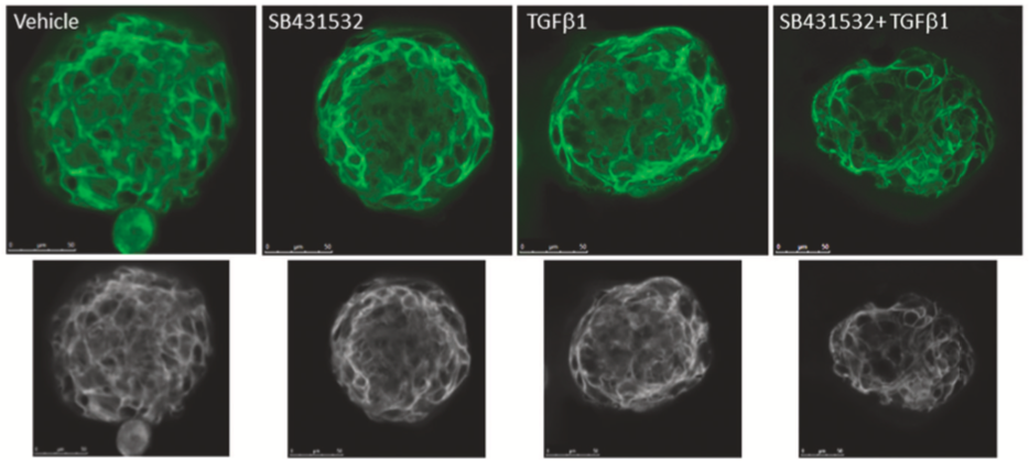
We utilized esophageal biopsies and fibroblasts from TT-genotype EoE children to understand if TGFβ1 influenced fibroblast and epithelial cell function in vivo. Genotype TT EoE esophageal fibroblasts had higher baseline TGFβ1, collagen1α1, periostin, and MMP2 (p < 0.05) gene expression and distinct contractile properties compared with CC genotype (n = 6 subjects per genotype). In vitro TGFβ1 exposure caused greater induction of target gene expression in genotype CC fibroblasts (p < 0.05). Esophageal biopsies from TT-genotype subjects had significantly less epithelial membrane-bound E-cadherin (p < 0.01) and wider cluster distribution at nanometer resolution. TGFβ1 treatment of stratified primary human esophageal epithelial cells and spheroids disrupted transepithelial resistance (p < 0.001) and E-cadherin localization (p < 0.0001). A TGFβ1-receptor-I inhibitor improved TGFβ1-mediated E-cadherin mislocalization. These data suggest that EoE severity can depend on genotypic differences that increase in vivo exposure to TGFβ1. TGFβ1 inhibition may be a useful therapy in subsets of EoE patients.
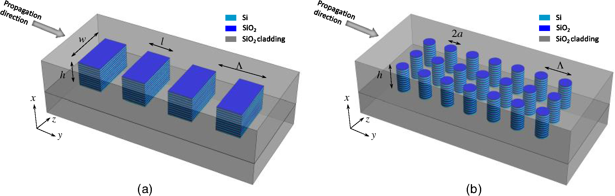
We proposed and systematically analyzed the propagation properties of periodic segmented waveguides and nanowire waveguides where the segments and nanowires have been considered to be composed of multilayers of silicon and silica with subwavelength thickness. We demonstrated, through a comprehensive number of numerical simulations involving modal analysis, that the artificial uniaxial negative anisotropy introduced by the multilayered segments or nanowire can be used to engineer waveguides with independent polarization propagation characteristic over the entire band of optical communication frequencies.
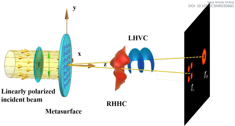
Similar to amplitude and phase, optical spin plays an important and nontrivial role in optics, which have been widely demonstrated in wavefront engineering, creation of new optical components, and sensitive optical metrology. In this work, we propose and experimentally demonstrate a new type of spin controlled wavefront shaping metasurface. The proposed geometric phase metasurface is designed by employing the integrated and interleaved structures to independently control the left and right-handed spin components. As an exemplary demonstration, our experimental results show that such a composite metasurface can convert a plane wave into a vortex beam and a Hermite beam for left-handed and right-handed polarized light, respectively. Because such metasurface is made by non-resonance dielectric structures, it can work for broadband frequencies with very low dispersion. The proposed metasurface is fabricated by the laser writing method in a transparent glass with a low-cost, which avoids the typical high-resolution lithography process. This spin dependent broadband wavefront shaping metasurface may find potential applications in optical communications, information processing, and optical metrology.
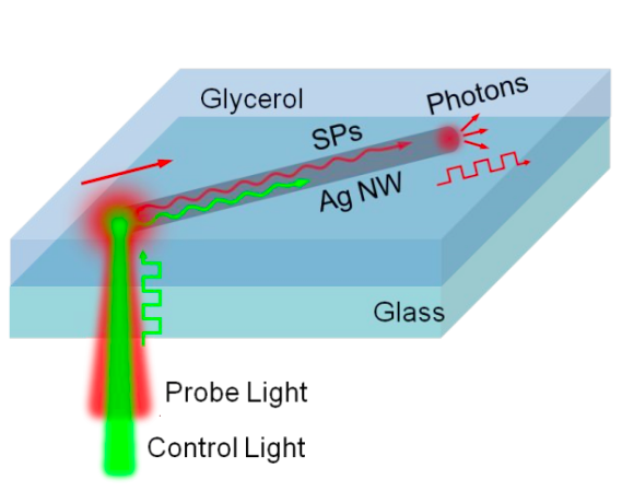
Nanoplasmonic devices have received much attention in recent years due to their ability to confine light beyond the diffraction limit. Manipulating the propagation of surface plasmons (SPs) is of vital importance for the creation of nanometer-scale integrated photonic devices. In this work we exploit the photothermal property of a silver nanowire (NW) to optically modulate the propagation of SPs on it. Under the excitation of a control laser beam, the rise of local temperature induced by the photothermal effect of silver NW results in the dramatic increase or decrease of the intensity of the transmitted SPs generated by a probe laser beam, depending on the Fabry-Pérot resonance conditions of the SPs on the NW. The amplitude of the photothermal modulation depth is found to be strongly dependent on the focal positions, polarizations, and power of the control beam. The simulations reveal that the high modulation depth at the NW end is mainly caused by the additional heat generated by the propagating SPs on the NW. The analytical solutions for the transmissivity and modulation depth are presented. Both numerical simulations and theoretical analysis agree well with the experimental results. Our work provides not only a new kind of all-optical modulation method for the propagating SPs in ultra-compact plasmonic devices, but also the basic understanding about the influence of environmental temperature on the propagating SPs.
Localized plasmonic structured illumination microscopy (LPSIM) is a super-resolution fluorescent microscopy method to image samples at a high speed with a wide field of view and low phototoxicity. Here we propose a methodology to extend the resolution capability of LPSIM by shifting spatial frequencies farther away from the diffraction-limited cutoff frequency with a plasmonic nano-array. We analyze the performance and accuracy of image reconstruction by using simulations of standard structured illumination microscopy (SIM) and blind-LPSIM. LPSIM experiments were also performed by using various LPSIM substrates and different microscope objectives. The experiments and simulations show that by shifting spatial frequencies farther away, resolution improvement can be extended up to 5 times beyond the diffraction limit with minimal deformation and artifacts in the reconstructed image.
Edge detection is a fundamental tool in image processing, computing, and machine vision. Compared with digital processes, optical analog approaches show enormous advantages owing to its intrinsic parallel nature for high-speed operation. Recently, optical metamaterials and metasurfaces have performed edge detection via analog spatial differentiation, which shows superior integration capability compared with the traditional bulky system. Unfortunately, experimental realization of optical-edge detection with metamaterials and metasurfaces remains challenging based on previous theoretical proposals. Here, we demonstrated a mechanism to realize an optical spatial differentiator consisting of a designed metasurface sandwiched by two orthogonally aligned linear polarizers. This approach relies on spin-orbit interaction of light and the metasurface, showing versatile edge-detection capability with exceptional quality.
Photodetectors made of amorphous materials enable low cost optical imaging and communications over non-semiconductor platforms. The key challenges are to improve efficiency, sensitivity, and frequency response. Using the localized surface plasmon resonance (LSPR) effect and an efficient carrier multiplication process, cycling excitation process (CEP), the plasmonically enhanced amorphous silicon photodetector (PEASP) with a thin (60 nm) absorption layer achieves a high external quantum efficiency with a record fast impulse response of 170 ps (FWHM). This approach offers the possibility of making detectors out of amorphous material for high frame rate imaging and optical communications in spite of the material's low carrier mobility.
This work studies organic bulk heterojunction photodiodes with a wide spectral range capable of imaging out to 1.3 um in the shortwave infrared. Adjustment of the donor-to-acceptor (polymer:fullerene) ratio shows how blend composition affects the density of states (DOS) which connects materials composition and optoelectronic properties and provides insight into features relevant to understanding dispersive transport and recombination in the narrow bandgap devices. Capacitance spectroscopy and transient photocurrent measurements indicate the main recombination mechanisms arise from deep traps and poor extraction from accumulated space charges. The amount of space charge is reduced with a decreasing acceptor concentration; however, this reduction is offset by an increasing trap DOS. A device with 1:3 donor-to-acceptor ratio shows the lowest density of deep traps and the highest external quantum efficiency among the different blend compositions. The organic photodiodes are used to demonstrate a single-pixel imaging system that leverages compressive sensing algorithms to enable image reconstruction.
High-resolution multipoint simultaneous structure-function analysis is becoming of great interest in a broad spectrum of fields for deciphering multiscale dynamics, especially in biophysics and materials science. However, current techniques are limited in terms of versatility, resolution, throughput, and biocompatibility. Here, a multifunctional imaging platform is introduced that shows high sensitivity, minimum cross-talk, and a variety of probe-based sensing. This is demonstrated by parallel multiparametric studies in air and liquid, including mechanical wave propagation in a soft polymer film, imaging of live neurons, and cooperative activities of living coupled cardiac muscle cells. As an experimental demonstration of array atomic force microscopy for multiparametric analysis in dynamic systems this work sheds light on the study of emergent properties in wide-ranging fields.
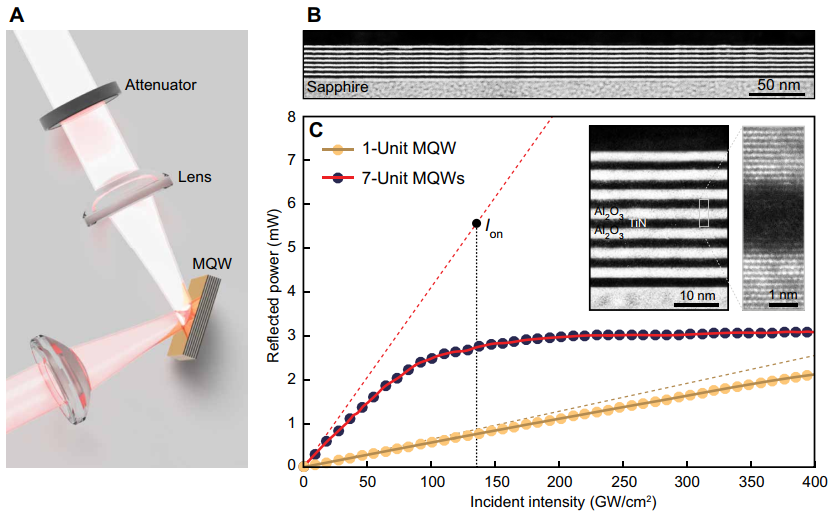
Here, we introduce a metal/dielectric heterostructured platform, i.e., TiN/Al2O3 epitaxial multilayers, to overcome that limitation. This platform has an extremely high χ(2) of approximately 1500 pm/V at NIR frequencies. By combining the aforementioned heterostructure with the large electric field enhancement afforded by a nanostructured metasurface, the power efficiency of second harmonic generation (SHG) achieved 10-4 at an incident pulse intensity of 10 GW/cm2, which is an improvement of several orders of magnitude compared to that of previous demonstrations from nonlinear surfaces at similar frequencies. The proposed quantum-engineered heterostructures enable efficient wave mixing at visible/NIR frequencies into ultracompact nonlinear optical devices.
A key challenge for optical circuits is the ability to integrate nonlinear optical signal processing components such as optical modulators and frequency mixers at the chip scale. Optical antennas that focus light into nanoscale volumes can be utilized to shrink the footprint and increase the efficiency of these components. Multiresonant antennas that enhance both optical absorption and emission process are recently demonstrated to enable efficient nonlinear frequency conversion at the nanoscale and are promising as structures for second harmonic generation (SHG) and upconversion. Here, the ability of colloidal metasurfaces fabricated by self-assembly as on-chip platforms for enhanced SHG is demonstrated. These metasurfaces exhibit high spatial overlap of multiple surface plasmon modes whose frequencies can be independently tuned through appropriate design of colloidal and metasurface geometries. It is demonstrated that these bottom-up structures rival lithographic nonlinear optical antennas in SHG efficiency, suggesting the potential for these colloidal metasurfaces in integrated on-chip architectures.
Nanopatterned multilayer hyperbolic metamaterials (HMMs) with engineerable material property are promising in enhancing spontaneous emission rates at desired frequencies with improved far-field radiative power. In this work, the authors study the optimization process for spontaneous emission enhancement by using nanopatterned HMMs. By theoretically investigating the Purcell effect on HMMs compared with traditional metals, the authors choose better material combinations for stronger Purcell enhancement. Different decay channels in the HMM are analyzed against the emitter distance and their wavelengths. Systematic optimization of achieving large emission intensity is demonstrated by comparing performance of nanopatterned HMMs with different geometry parameters. The promise in achieving light emission with both high decay rates and brightness has various potential applications including light-emitting devices, single molecule detection, and surface-enhanced Raman scattering.
An optical metamaterial is capable of manipulating light in nanometer scale that goes beyond what is possible with conventional materials. Taking advantage of this special property, metamaterial-assisted illumination nanoscopy (MAIN) possesses tremendous potential to extend the resolution far beyond conventional structured illumination microscopy. Among the available MAIN designs, hyperstructured illumination that utilizes strong dispersion of a hyperbolic metamaterial (HMM) is one of the most promising and practical approaches, but it is only theoretically studied. In this paper, we experimentally demonstrate the concept of hyperstructured illumination. A ~80 nm resolution has been achieved in a well-known Ag/SiO2 multilayer HMM system by using a low numerical aperture objective (NA = 0.5), representing a 6-fold resolution enhancement of the diffraction limit. The resolution can be significantly improved by further material optimization.
A large-scale sub-5 nm nanofabrication technique is developed based on double layer anodized aluminium oxide (AAO) porous membrane masking. This technique also provides a facile route to form multilayer nano-arrays (metal nanoarrays sandwiched by AAO membranes), which is very challenging for other techniques. The preserved AAO layers as the support for the second/third layer of the metal arrays provide a high-refractive index background for the multilayer metal arrays. This background concentrates the local E-field more significantly and results in a much higher Surface-Enhanced Raman Spectroscopy (SERS) signal than single layer metal arrays. This technique may lead to the advent of an inexpensive, reproducible, highly sensitive SERS substrate.
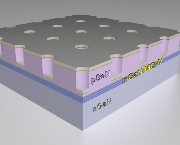
We design, fabricate and analyze a nanostructured plasmonic light emitting diode (LED) that simultaneously increases the modulation speed and radiative efficiency, compared to conventional LEDs and unpatterned plasmonic LEDs respectively. Our structure, optimized to ensure its integrability with electrical contacts, couples an InGaN/GaN blue LED with a Ag nanohole grating. Through spatio-temporally resolved photoluminescence measurements, we determine a 40-fold decrease in spontaneous emission lifetime, which sets an upper bound to the direct modulation bandwidth in the GHz regime. Additionally, through careful optimization of the plasmonic nanohole grating, we demonstrate a 10-fold increase in outcoupling efficiency relative to an LED with an unstructured plasmonic film. Our work bridges the plasmonic metamaterial and III-nitride semiconductor communities, laying the groundwork for high-speed, high-efficiency blue plasmonic LEDs for applications in visible light communication and beyond.
Localized plasmonic structured illumination microscopy (LPSIM) provides multicolor wide-field super-resolution imaging with low phototoxicity and high-speed capability. LPSIM utilizes a nanoscale plasmonic antenna array to provide a series of tunable illumination patterns beyond the traditional diffraction limit, allowing for enhanced resolving powers down to a few tens of nanometers. Here, we demonstrate wide-field LPSIM with 50 nm spatial resolution at video rate speed by imaging microtubule dynamics with low illumination power intensity. The design of the LPSIM system makes it suitable for imaging surface effects of cells and tissues with regular sample preparation protocols. LPSIM can be extended to much higher resolution, representing an excellent technology for live-cell imaging of protein dynamics and interactions.
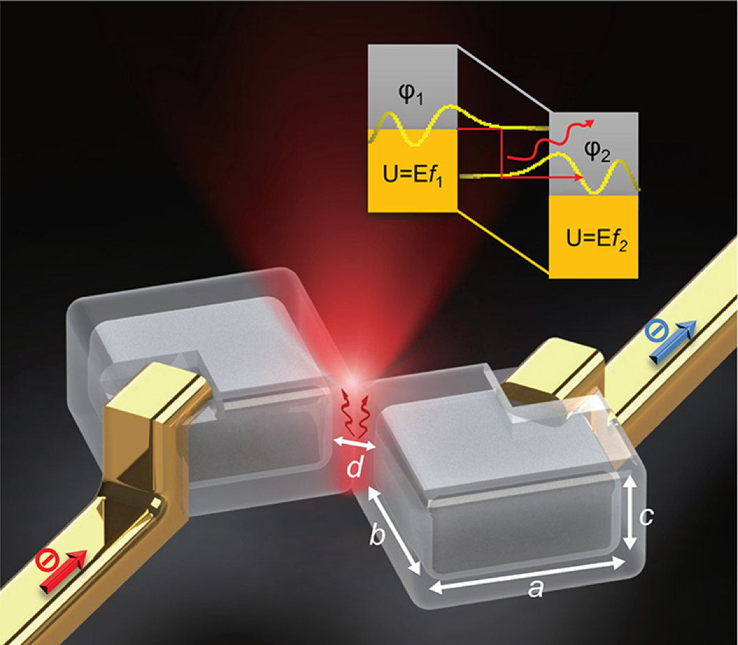
Light emission from biased tunnel junctions has recently gained much attention owing to its unique potential to create ultracompact optical sources with terahertz modulation bandwidth. The emission originates from an inelastic electron tunnelling process in which electronic energy is transferred to surface plasmon polaritons and subsequently converted to radiation photons by an optical antenna. Because most of the electrons tunnel elastically, the emission efficiency is typically about 10-5-10-4. Here, we demonstrate efficient light generation from enhanced inelastic tunnelling using nanocrystals assembled into metal-insulator-metal junctions. The colour of the emitted light is determined by the optical antenna and thus can be tuned by the geometry of the junction structures. The efficiency of far-field free-space light generation reaches ~2%, showing an improvement of two orders of magnitude over previous work. This brings on-chip ultrafast and ultra-compact light sources one step closer to reality.
Structured illumination microscopy (SIM) is one of the most versatile super-resolution techniques. Compared with other methods, SIM has shown its advantages in high temporal resolution and low photodamage, but it only has a 2-fold increase in resolution. We review the recent developments of metamaterial assisted illumination nanoscopes (MAIN), which combines near-field patterned illumination generated by metamaterials to extend the resolution of SIM. MAIN addresses three of the most important imaging aspects simultaneously: resolution, frame rate, and phototoxicity opening up tremendous new opportunities for future developments and applications.
Organic-inorganic hybrid perovskites have demonstrated tremendous potential for the next-generation electronic and optoelectronic devices due to their remarkable carrier dynamics. Current studies are focusing on polycrystals, since controlled growth of device compatible single crystals is extremely challenging. Here, the first chemical epitaxial growth of single crystal CH3NH3PbBr3 with controlled locations, morphologies, and orientations, using combined strategies of advanced microfabrication, homoepitaxy, and low temperature solution method is reported. The growth is found to follow a layer-by-layer model. A light emitting diode array, with each CH3NH3PbBr3 crystal as a single pixel, with enhanced quantum efficiencies than its polycrystalline counterparts is demonstrated.
We demonstrate hyperbolic metamaterials (HMMs) on a curved surface for an efficient outcoupling of nonradiative modes, which lead to an enhanced spontaneous emission. Those high-wavevector plasmonic modes can propagate along the curved structure and emit into the far field, realizing a directional light emission with maximal fluorescent intensity. Detailed simulations disclose a high Purcell factor and a spatial power distribution in the curved HMM, which agrees with the experimental result. Our work presents remarkable enhancing capability in both the Purcell factor and emission intensity, which could suggest a unique structure design in metamaterials for potential application in, e.g., high-speed optical sensing and communications.
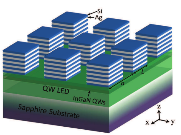
Here, nanopatterned Ag-Si multilayer HMMs are utilized for enhancing spontaneous carrier recombination rates in InGaN/GaN QWs. An enhancement of close to 160-fold is achieved in the spontaneous recombination rate across a broadband of working wavelengths accompanied by over tenfold enhancement in the QW peak emission intensity, thanks to the outcoupling of dominating HMM modes. The integration of nanopatterned HMMs with InGaN QWs will lead to ultrafast and bright QW LEDs with a 3 dB modulation bandwidth beyond 100 GHz for applications in high-speed optoelectronic devices, optical wireless communications, and light-fidelity networks.
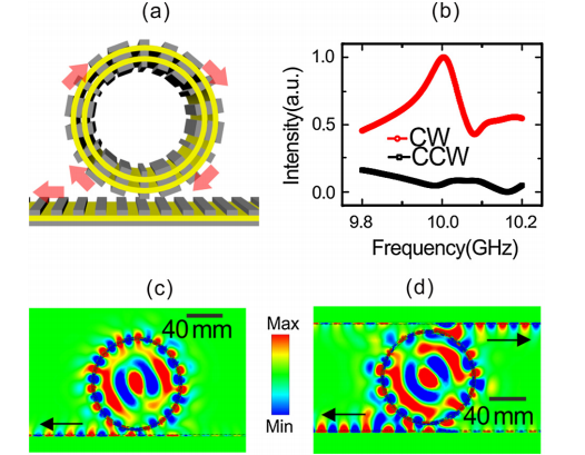
Optical microcavities with whispering-gallery modes (WGMs) have been indispensable in both photonic researches and applications. Besides, metasurfaces, have attracted much attention recently due to their strong abilities to manipulate electromagnetic waves. Here, combining these two optical elements together, we show a tubular cavity can convert input propagating cylindrical waves into directed localized surface waves (SWs), enabling the circulating like WGMs along the wall surface of the designed tubular cavity. Finite element method (FEM) simulations demonstrate that such near-field WGM shows both large chirality and high local field. This work may stimulate interesting potential applications in e.g. directional emission, sensing, and lasing.
A nonlinear metasurface is demonstrated numerically based on the recently developed quantum-sized gold film. The active functionality of the metasurface is realized by varying the incident optical power through the ultrahigh Kerr nonlinearity of the quantum-sized gold films. In the low power region, the device acts as a normal reflecting surface, while it becomes a phase grating with most energy in the ±1 diffraction modes when the optical power increases and the nonlinear effect plays a dominating role. Unlike previously demonstrated nonlinear metasurfaces focusing on nonlinear frequency generation, the functionality of our device may be modulated by the power of incident light. As the first nonlinear metasurface that is based on optical Kerr nonlinearity, our design may lead to various applications, such as optical limiters and tunable phase gratings.
Hyperbolic metamaterials (HMM) can be used to control light propagations in emerging meta-devices and thus lead to various functionalities (e.g., hyperlens and cloaking devices). Here we propose a kind of exotic tubular cavity by using multilayered HMM, which contrasts with traditional materials with elliptical dispersion. In such tubular microcavities, the calculations reveal that they have anomalous scaling laws, such as that the higher-order resonance mode oscillates at a longer wavelength and the resonant wavelengths hold their positions with changing the tube wall thickness and diameter. These findings can help the understanding of tubular metamaterials and could inspire interesting optical experiments and metadevices.
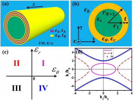
Meta-lens represents a promising solution for optical communications and information processing owing to its miniaturization capability and desirable optical properties. Here, spin Hall meta-lens is demonstrated to manipulate photonic spin-dependent splitting induced by spin-orbital interaction in transverse and longitudinal directions simultaneously at visible wavelengths, with low dispersion and more than 90% diffraction efficiency. The broadband dielectric spin Hall meta-lens is achieved by integrating two geometric phase lenses with different functionalities into one single dynamic phase lens, which manifests the ultracompact, portable, and polarization-dependent features. The broadband spin Hall meta-lens may find important applications in imaging, sensing, and multifunctional spin photonics devices.
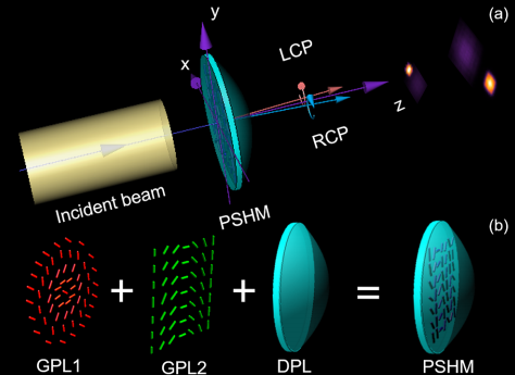
Three-dimensional (3D) imaging at the nanoscale is a key to understanding of nanomaterials and complex systems. We demonstrate plasmonic Brownian microscopy (PBM) as a way to improve the imaging speed of SPM. Unlike photonic force microscopy where a single trapped particle is used for a serial scanning, PBM utilizes a massive number of plasmonic nanoparticles (NPs) under Brownian diffusion in solution to scan in parallel around the unlabeled sample object. The motion of NPs under an evanescent field is three-dimensionally localized to reconstruct the super-resolution topology of 3D dielectric objects. Our method allows high throughput imaging of complex 3D structures over a large field of view, even with internal structures such as cavities that cannot be accessed by conventional mechanical tips in SPM.
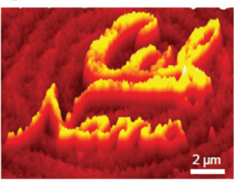
We present a new far-field super-resolution imaging approach called compressive spatial to spectral transformation microscopy (CSSTM). The transformation encodes high-resolution spatial information to a spectrum through illuminating sub-diffraction-limited and wavelength-dependent patterns onto an object. The object is reconstructed from scattering spectrum measurements in the far field. The resolution of the CSSTM is mainly determined by the materials used to perform the spatial-spectral transformation. As an example, we numerically demonstrate sub-15nm resolution by using a practically achievable Ag/SiO2 multilayer hyperbolic metamaterial.
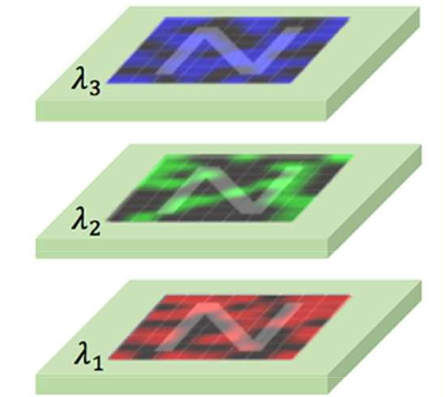
Localized plasmonic structured illumination microscopy (LPSIM) is a recently developed super resolution technique that demonstrates immense potential via arrays of localized plasmonic antennas. Microlens microscopy represents another distinct approach for improving resolution by introducing a spherical lens with a large refractive index to boost the effective numerical aperture of the imaging system. In this paper, we bridge together the LPSIM and optically trapped spherical microlenses, for the first time, to demonstrate a new super resolution technique for surface imaging. By trapping and moving polystyrene and TiO2 microspheres with optical tweezers on top of a LPSIM substrate, the new imaging system has achieved a higher NA and improved resolution.
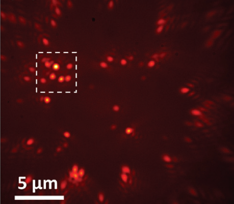
A novel method is presented to outcouple high spatial frequency (large-k) waves from hyperbolic metamaterials (HMMs) without the use of a grating. This approach relies exclusively on dispersion engineering, and enables preferential power extraction from the top or from the side of a HMM. A 6-fold increase in laterally extracted power is predicted for a dipole-HMM system with a Ag/Si ML operating at λ = 530 nm, when metallic filling ratio is changed from an unoptimized to the optimized one. This new design concept supports the cost-effective mass production of high-speed HMM optical transmitters.
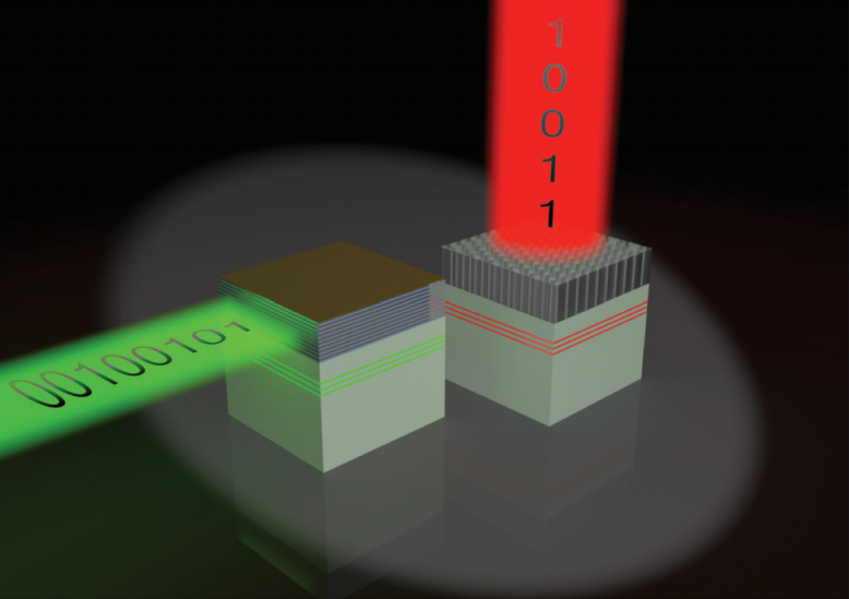
Super-resolution imaging methods such as structured illumination microscopy and others have offered various compromises between resolution, imaging speed, and biocompatibility. Here we experimentally demonstrate a physical mechanism for super-resolution that offers advantages over existing technologies. Using finely structured, resonant, and controllable near-field excitation from localized surface plasmons in a planar nanoantenna array, we achieve wide-field surface imaging with resolution down to 75 nm while maintaining reasonable speed and compatibility with biological specimens.
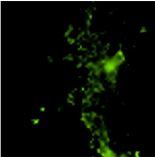
Here we present a nanosystem, a superlattice monolayer formed by sub-10 nm gold nanoparticles. Plasmon resonances are spectrally well-separated from interband transitions, while exhibiting clearly distinguishable blueshifts compared to predictions by the classical local-response model. Our far-field spectroscopy was performed by a standard optical transmission and reflection setup, and the results agreed excellently with the hydrodynamic nonlocal model, opening a simple and widely accessible way for addressing quantum effects in nanoplasmonic systems.
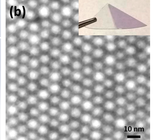
Here, a class of materials, transferrable hyperbolic metamaterial particles (THMMP), is introduced. When closely packed, these materials show broadband, selective, omnidirectional, perfect absorption. This is demonstrated with nanotubes made on a silicon substrate that exhibit near-perfect absorption at telecommunication wavelengths even after being transferred to a mechanically flexible, visibly transparent polymer.
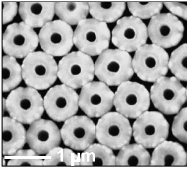
Here, we demonstrate a novel method for compact spectrometry that uses an array of etalons to perform spectral encoding, and uses a reconstruction algorithm to recover the incident spectrum. This spectrometer has the unique capability for both high resolution and a large working bandwidth without sacrificing sensitivity, and we anticipate that its simplicity makes it an excellent candidate whenever a compact, robust, and flexible spectrometry solution is needed.
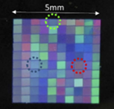
Using an unconventional multilayer architecture, we demonstrate luminescent hyperbolic metasurfaces, wherein distributed semiconducting quantum wells display extreme absorption and emission polarization anisotropy. Through normally incident micro-photoluminescence measurements, we observe absorption anisotropies greater than a factor of 10 and degree-of-linear polarization of emission >0.9. We observe the modification of emission spectra and, by incorporating wavelength-scale gratings, show a controll ed reduction of polarization anisotropy. Finally, we experimentally demonstrate >350% emission intensity enhancement relative to the bare semiconducting quantum wells.
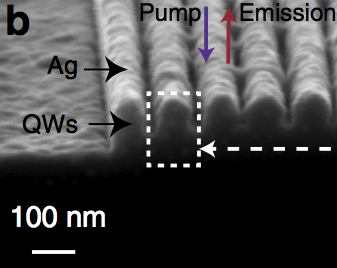
A novel DMBT-concept tandem applicator that enables enhanced capacity to sculpt the 3D dose distributions in HDR brachytherapy was proposed in 2014. Subsequently, a comprehensive comparative planning study was performed on 45 cervical cancer patients, enrolled in the EMBRACE trial, treated with various intracavitary and intracavitary-interstitial techniques. All cases were replanned with an in-house-developed inverse optimization code. The proposed applicator was found to enhance the plan quality across various clinical scenarios.
Here, we demonstrate fabrication of highly flexible and stretchable wire grid polarizers (WGPs) by printing bottom-up grown Ge or Ge/Si core/shell nanowires (NWs) on device substrates in a highly dense and aligned fashion. The maximum contrast ratio of 104 between transverse electric (TE) and transverse magnetic (TM) fields and above 99% (maximum 99.7%) of light blocking efficiency across the visible spectrum range are achieved. Further systematic analyses are performed both in experimental and numerical models to reveal the correspondence between physical factors (coverage ratio of NW arrays and diameter) and polarization efficiency.
Here we study the optical nonlinear properties of a nanometre scale gold quantum well by using the z-scan method and nonlinear spectrum broadening technique. The quantum size effect results in a giant optical Kerr susceptibility, which is four orders of magnitude higher than the intrinsic value of bulk gold and several orders larger than traditional nonlinear media. Such high nonlinearity enables efficient nonlinear interaction within a microscopic footprint, making quantum metallic films a promising candidate for integrated nonlinear optical applications.
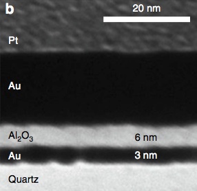
The conventional optical microscope is an inherently two-dimensional (2D) imaging tool. In this paper, we present a 3D optical microscopy method based upon simultaneously illuminating and detecting multiple focal planes. This is implemented by adding two diffractive optical elements to modify the illumination and detection optics. We demonstrate that the image quality of this technique is comparable to conventional light sheet fluorescent microscopy with the advantage of the simultaneous imaging of multiple axial planes and reduced number of scans required to image the whole sample volume.
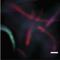
For a normal distribution of free-electron nanoparticles, and within the simple nonlocal hydrodynamic Drude model, both the nonlocal blueshift and the plasmon linewidth are shown to be considerably affected by ensemble averaging. Size-variance effects tend however to conceal nonlocality to a lesser extent when the homogeneous size-dependent broadening of individual nanoparticles is taken into account , either through a local size-dependent damping model or through the Generalized Nonlocal Optical Response theory. The role of ensemble averaging is further explored in realistic distributions of isolated or weakly-interacting noble-metal nanoparticles, as encountered in experiments, while an analytical expression to evaluate the importance of inhomogeneous broadening through measurable quantities is developed.
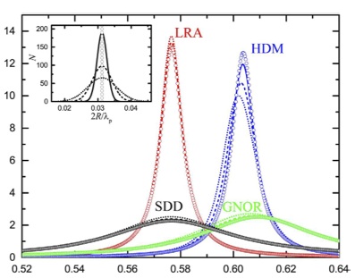
In this work, we have developed tandem-structured solar absorbing layers with CuFeMnO4 and CuCr2O4 black oxide nanoparticles (NPs). These tandem structures exhibited a remarkably high solar-to-thermal conversion efficiency, or figure of merit (FOM), of 0.903, under the condition of 750oC operating temperature and a solar concentration ratio of 1000. More importantly, the coating showed unprecedented durability, as demonstrated from long-term isothermal annealing at 750oC in air as well as rapid thermal cycling between room temperature and 750oC.
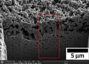
One potential way to improve the imaging speed of CCD cameras is with compressive sensing (CS), a technique that allows for a reduction in the number of measurements needed to record an image. However, most CS imaging methods require spatial light modulators (SLMs), which are subject to mechanical speed limitations. Here, we demonstrate an etalon array based SLM without any moving elements that is unconstrained by either mechanical or electronic speed limitations. This novel spectral resonance modulator (SRM) shows great potential in an ultrafast compressive single pixel camera.

In this work, we demonstrate the two-photon fluorescence of covellite-phase copper sulfide nanodisks and investigate the role of the surface plasmon resonance on emission. Using selenium doping, we blue-shift the plasmon resonance toward the two-photon absorption edge. We observed a 3-fold enhancement of emission in these samples and report two-photon action cross sections that are an order of magnitude greater than conventional fluorophores. These nanomaterials offer a novel “all-in-one” platform for engineering plasmon-exciton coupling in the absence of a physical or chemical interface.
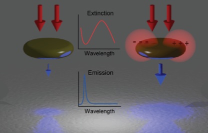
Aluminum-doped zinc oxide (AZO) is a tunable low-loss plasmonic material capable of supporting dopant concentrations high enough to operate at telecommunication wavelengths. Here a simple procedure is devised to tune the optical constants of AZO and enable plasmonic activity at 1550 nm with low loss. The high-quality AZO is then used to make a layered AZO/ZnO structure that displays negative refraction in the telecommunication wavelength region due to hyperbolic dispersion. Finally, a novel synthetic scheme is demonstrated to create AZO embedded nanowires in ZnO, which also exhibits hyperbolic dispersion.
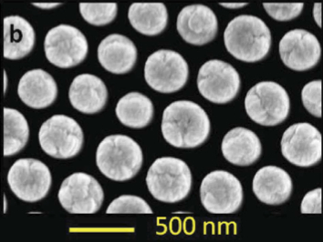
Based on Mie scattering theory, we propose a tubular metamaterial device for liquid sensing, which utilizes anisotropic metamaterials with hyperbolic dispersion called indefinite media (IM). Compared with traditional dielectric media (DM), the IM tubular cavity exhibits a higher sensitivity (S), which is close to that of a metal tubular cavity. However, compared with metal media, such an IM cavity can achieve higher quality (Q) factors similar to the DM tubular cavity. Therefore, the IM tubular cavity can offer the highest figures of merit for the sensing performance among the three types of materials.
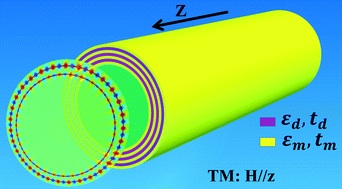
The optical properties of thin gold films with thickness varying from 2.5 nm to 30 nm are investigated. Due to the quantum size effect, the optical constants of the thin gold film deviate from the Drude model for bulk material as film thickness decreases, especially around 2.5 nm, where the electron energy level becomes discrete. A theory based on the self-consistent solution of the Schrodinger equation and the Poisson equation is proposed and its predictions agree well with experimental results.
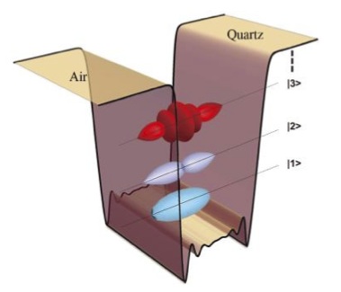
In this paper, we prepared a novel structure to enhance the electroluminescence intensity from Si quantum dots/SiO2 multilayers. An amorphous Si/SiO2 multilayer film was fabricated by plasma-enhanced chemical vapor deposition on a Pt nanoparticle (NP)-coated Si nanopillar array substrate. By thermal annealing, an embedded Si quantum dot (QDs)/SiO2 multilayer film was obtained. The result shows that electroluminescence intensity was significantly enhanced. And, the turn-on voltage of the luminescent device was reduced to 3V.
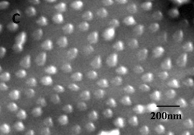
We report successful growth of a uniform and scalable nanocomposite film of Fe2O3 nanorods (NRs) and NiOx nanoparticles (NPs), their properties and application for enhanced solar water reduction in neutral pH water on the surface of p-Si photocathodes.
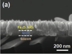
In this letter, we numerically demonstrate a hyperlens with unprecedented radial-resolution at 5 nm scale for both imaging and lithography applications. Both processes are shown to have accuracy that surpasses the Abbe diffraction limit in the radial direction, which has potential applications for 3D imaging and lithography. Design optimization is discussed with regards to several important hyperlens parameters.
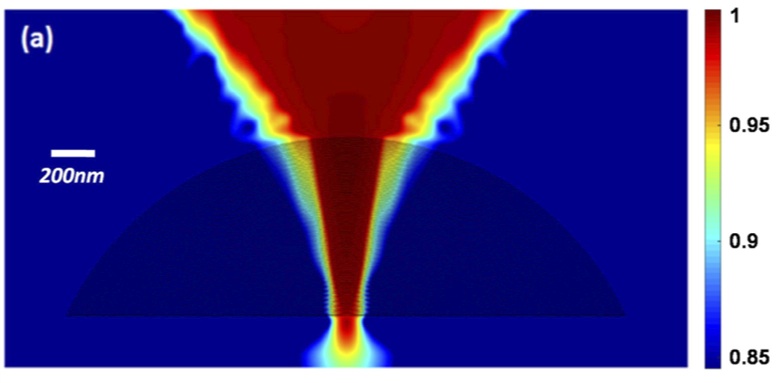
In contrast to strong plasmonic scattering from metal particles or structures in metal films, we show that patterns of arbitrary shape fabricated out of multilayer hyperbolic metamaterials become invisible within a chosen band of optical frequencies. This is due to anomalously weak scattering when the in-plane permittivity of the multilayer hyperbolic metamaterials is tuned to match with the surrounding medium. This anomalously weak scattering is insensitive to pattern sizes, shapes, and incident angles, and has potential applications in scattering cross-section engineering, optical encryption, low-observable conductive probes, and optoelectric devices.
We present a far-field super-resolution imaging scheme based on coherent scattering under a composite photonic-plasmonic structured illumination. The 4-fold super-resolution power of the scheme, able to resolve 60 nm feature sizes at the operating wavelength, is demonstrated against both Abbe's (imaging a single object) and Rayleigh's (imaging two closely spaced objects) criteria.
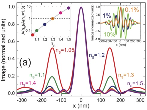
In this work, a black oxide material, made of cobalt oxide nanoparticles, is synthesized and utilized as a high-temperature solar absorbing material. After the surface modification of cobalt oxide coating, we achieved a high thermal efficiency of 88.2%. More importantly, the coating shows no degradation after 1000-h annealing at 750oC in air, while the existing commercial light absorbing coating was reported to degrade by long- term exposure at high temperature. Our findings suggest that the materials and processes developed here are promising for solar absorbing coating for future high-temperature CSP systems.
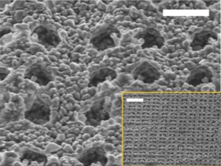
This review aims at providing a comprehensive and updated picture of the field of hyperbolic metamaterials, from the foundations to the most recent progresses and future perspectives. The topics discussed embrace theoretical aspects, practical realization and key challenges for applications such as imaging, spontaneous emission engineering, thermal, active and tunable hyperbolic media.
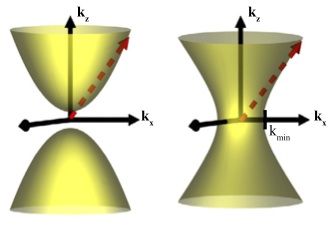
We report novel tandem structures combing two different materials with complementary optical properties and microstructures: copper oxide (CuO) nanowires (NWs) and cobalt oxide (Co3O4) nanoparticles (NPs). Tandem structures of spectrally selective coating (SSC) layer are built with three different methods: spray-coating, dip-coating of cobalt oxide NPs into copper oxide NWs forest, and transferring of copper oxide NWs layer onto cobalt oxide NPs layer. Our results demonstrate the efficacy of using novel tandem structures for enhanced light absorption of solar spectrum, which will find broad applications in solar energy conversion.